
Image not available
Illustrative purposes only

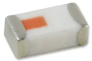
5400AT18A1000E
CHIP ANTENNA, 4.9-5.9GHZ, 3.2X1.6X1.3MM
⚠️ Reference pricing provided. In case of supply shortages, we will connect you with our trusted procurement partners to ensure your project's continuity.
- Manufacturer: JOHANSON TECHNOLOGY
- Product type: Antennas - Single Band Chip
- Antenna Type:-; Operating Frequency:5900MHz; Antenna Connector:-; Antenna Cable Length:-; Transmit Power:-; Antenna Polarisation:-; Gain:-2.5dB; Antenna Mounting:SMD; Product Rang
- SVHC: No SVHC (17-Jan-2023)
- Product Range: -
- Antenna Mounting: SMD
- Centre Frequency: -
- Antenna Case Size: 3.2mm x 1.6mm x 1.3mm
- Operating Frequency: 5900MHz
| Delivery and price | |
|---|---|
| Units per pack | 3000 |
| Price | 0.132 € |
| Current stock | 10+ |
| Lead time | 30 days |
Datasheet

## **x2y® fIlter & decouPlIng caPacItors**

X2Y[®] filter capacitors employ a unique, patented low inductance design featuring two balanced capacitors that are immune to temperature, voltage and aging performance differences.

These components offer superior decoupling and EMI filtering performance, virtually eliminate parasitics, and can replace multiple capacitors and inductors saving board space and reducing assembly costs.

## _adVantageS applicationS_

- One device for EMI suppression or decoupling

   - Amplifier FIlter & Decoupling

   - High Speed Data Filtering

- Replace up to 7 components with one X2Y

   - EMC I/O Filtering

- Differential and common mode attenuation

|• Differential and common mode attenuation<br>• Matched capacitance line to ground, both lines<br>• Low inductance due to cancellation effect<br>• EMC I/O Filtering<br>• FPGA / ASIC / µ-P  Decoupling<br>• DDR Memory Decoupling<br>EMI Filtering<br>(1 Y-Cap.)<br><10pF<br>10pF<br>22pF<br>27pF<br>33pF<br>47pF<br>100pF<br>220pF<br>470pF<br>1000pF<br>1500pF<br>2200pF<br>4700pF<br>.010µF<br>.015µF<br>.022µF<br>.039µF<br>.047µF<br>0.10µF<br>0.18µF<br>0.22µF<br>0.33µF<br>0.40µF<br>0.47µF<br>1.0µF<br>Power Bypass<br>(2 Y-Caps.)<br><20pF<br>20pF<br>44pF<br>54pF<br>66pF<br>94pF<br>200pF<br>440pF<br>940pF<br>2000pF<br>3000pF<br>4400pF<br>9400pF<br>.020µF<br>.030µF<br>.044µF<br>.078µF<br>.094µF<br>0.20µF<br>0.36µF<br>0.44µF<br>0.68µF<br>0.80µF<br>0.94µF<br>2.0µF<br>SIZE<br>CAP.<br>CODE<br>XRX<br>100<br>220<br>270<br>330<br>470<br>101<br>221<br>471<br>102<br>152<br>222<br>472<br>103<br>153<br>223<br>393<br>473<br>104<br>184<br>224<br>334<br>404<br>474<br>105<br>0402 (X07)<br>NPO<br>50<br>50<br>50<br>50<br>50<br>50<br>50<br>X7R<br>50<br>50<br>50<br>50<br>50<br>50<br>16<br>0603 (X14)<br>NPO<br>100 100 100 100 100<br>50<br>50<br>50<br>X7R<br>100 100 100 100 100 100 100 100<br>50<br>25<br>25<br>16<br>10<br>10 <br>X5R<br>16<br>10<br>10<br>10<br>0805 (X15)<br>NPO<br>100 100 100 100 100 100 100<br>50<br>X7R<br>100 100 100 100 100 100 100 100<br>50<br>50<br>50<br>25<br>10<br>1206 (X18<br>NPO<br>VOLTAGE<br>RATINGS<br>6.3 = 6.3 VDC<br>10 = 10 VDC<br>16 = 16 VDC<br>25 = 25 VDC<br>50 = 50 VDC<br>100 = 100 VDC<br>500 = 500 VDC<br>100<br>X7R<br>100 100 100<br>100 100<br>16<br>16<br>10<br>1210 (X41)<br>X7R<br>500<br>100<br>100 100<br>25<br>16<br>1410 (X44)<br>X7R<br>500<br>100<br>1812 (X43)<br>X7R<br>500<br>100<br>eB~~EEE~~<br>~~EEE~~<br>~~EEE EEEEE~~<br>~~PEE~~<br>~~EEE EEE EEE EEEEEE~~<br>~~Pt~~<br>~~—~~<br>~~Pi] TTT~~ tT ~~TT~~ tT ~~TE EE EEE~~<br>~~P| TT~~ ~~| | |~~<br>~~Pi yee tT tt~~<br>~~_~~<br>~~PT TT tT TT TT ET ETT |~~<br>~~P| tt~~<br>~~|i~~<br>~~Seeeee~~<br>| ~~6c~~<br>~~—~~<br>~~a~~<br>~~PTT TT TT ET TT |~~<br>~~Pt T~~e<br>~~a~~<br>~~Pit |~~<br>~~— EEE PTT TTT ey ET~~<br>~~| |~~<br>~~**P**i yet~~<br>|<br>~~a~~<br>~~oe~~<br>~~en~~<br>~~ae~~<br>~~TT~~<br>~~Ti tt] aei~~<br>~~ee~~<br>~~en~~<br>~~ae~~<br>~~PTT TTT tt~~<br>~~| ae~~<br>~~eT~~<br>| ~~|~~<br>~~ae~~<br>~~en~~<br>~~ae~~<br>~~PTT TTT tt tt~~<br>~~Eee~~|• Differential and common mode attenuation<br>• Matched capacitance line to ground, both lines<br>• Low inductance due to cancellation effect<br>• EMC I/O Filtering<br>• FPGA / ASIC / µ-P  Decoupling<br>• DDR Memory Decoupling<br>EMI Filtering<br>(1 Y-Cap.)<br><10pF<br>10pF<br>22pF<br>27pF<br>33pF<br>47pF<br>100pF<br>220pF<br>470pF<br>1000pF<br>1500pF<br>2200pF<br>4700pF<br>.010µF<br>.015µF<br>.022µF<br>.039µF<br>.047µF<br>0.10µF<br>0.18µF<br>0.22µF<br>0.33µF<br>0.40µF<br>0.47µF<br>1.0µF<br>Power Bypass<br>(2 Y-Caps.)<br><20pF<br>20pF<br>44pF<br>54pF<br>66pF<br>94pF<br>200pF<br>440pF<br>940pF<br>2000pF<br>3000pF<br>4400pF<br>9400pF<br>.020µF<br>.030µF<br>.044µF<br>.078µF<br>.094µF<br>0.20µF<br>0.36µF<br>0.44µF<br>0.68µF<br>0.80µF<br>0.94µF<br>2.0µF<br>SIZE<br>CAP.<br>CODE<br>XRX<br>100<br>220<br>270<br>330<br>470<br>101<br>221<br>471<br>102<br>152<br>222<br>472<br>103<br>153<br>223<br>393<br>473<br>104<br>184<br>224<br>334<br>404<br>474<br>105<br>0402 (X07)<br>NPO<br>50<br>50<br>50<br>50<br>50<br>50<br>50<br>X7R<br>50<br>50<br>50<br>50<br>50<br>50<br>16<br>0603 (X14)<br>NPO<br>100 100 100 100 100<br>50<br>50<br>50<br>X7R<br>100 100 100 100 100 100 100 100<br>50<br>25<br>25<br>16<br>10<br>10 <br>X5R<br>16<br>10<br>10<br>10<br>0805 (X15)<br>NPO<br>100 100 100 100 100 100 100<br>50<br>X7R<br>100 100 100 100 100 100 100 100<br>50<br>50<br>50<br>25<br>10<br>1206 (X18<br>NPO<br>VOLTAGE<br>RATINGS<br>6.3 = 6.3 VDC<br>10 = 10 VDC<br>16 = 16 VDC<br>25 = 25 VDC<br>50 = 50 VDC<br>100 = 100 VDC<br>500 = 500 VDC<br>100<br>X7R<br>100 100 100<br>100 100<br>16<br>16<br>10<br>1210 (X41)<br>X7R<br>500<br>100<br>100 100<br>25<br>16<br>1410 (X44)<br>X7R<br>500<br>100<br>1812 (X43)<br>X7R<br>500<br>100<br>eB~~EEE~~<br>~~EEE~~<br>~~EEE EEEEE~~<br>~~PEE~~<br>~~EEE EEE EEE EEEEEE~~<br>~~Pt~~<br>~~—~~<br>~~Pi] TTT~~ tT ~~TT~~ tT ~~TE EE EEE~~<br>~~P| TT~~ ~~| | |~~<br>~~Pi yee tT tt~~<br>~~_~~<br>~~PT TT tT TT TT ET ETT |~~<br>~~P| tt~~<br>~~|i~~<br>~~Seeeee~~<br>| ~~6c~~<br>~~—~~<br>~~a~~<br>~~PTT TT TT ET TT |~~<br>~~Pt T~~e<br>~~a~~<br>~~Pit |~~<br>~~— EEE PTT TTT ey ET~~<br>~~| |~~<br>~~**P**i yet~~<br>|<br>~~a~~<br>~~oe~~<br>~~en~~<br>~~ae~~<br>~~TT~~<br>~~Ti tt] aei~~<br>~~ee~~<br>~~en~~<br>~~ae~~<br>~~PTT TTT tt~~<br>~~| ae~~<br>~~eT~~<br>| ~~|~~<br>~~ae~~<br>~~en~~<br>~~ae~~<br>~~PTT TTT tt tt~~<br>~~Eee~~|
|---|---|
||Contact factory for part combinations not shown.|
||Filtering capacitance is specified as Line-to-Ground  ( Terminal A or B to G)|
||Power Bypass capacitance is specified Power-to-Ground  (A + B to G)|
||Rated voltage is from line to ground in Circuit 1, power to ground in Circuit 2 .|
|_How to order X2y® capacitorS_<br>P/N written: 101X14W102MV4T||
|100<br>X14<br>W<br>102<br>M<br>V<br>4<br>T<br>VOLTAGE<br>SIZE<br>DIELECTRIC<br>CAPACITANCE<br>TOLERANCE<br>TERMINATION<br>MARKING<br>PACKING<br>Fo}<br>LJ<br>||<br>||<br>[|<br>| |<br>L]||
|6R3  =  6.3 V<br>X07=0402<br>N = NPO<br>1st two digits are signifi-<br>M =  ± 20%<br>V =  NI Barrier with 100%<br>4 = Unmarked<br>E<br>=Embossed 7”||
|100  =  10 V<br>160  =  16 V<br>250  =  25 V<br>500  =  50 V<br>101  =  100 V<br>501  =  500 V<br>X14=0603<br>X15=0805<br>X18=1206<br>X41=1210<br>X44=1410<br>X43=1812<br>W = X7R<br>X = X5R<br>cant; third digit denotes<br>number of zeros, R =<br>decimal.<br>102 = 1000 pF<br>104 = 0.10 µF<br>5R6 = 5.6pF<br>* D =  ± 0.50 pF<br>*Values < 10 pF only<br>Tin Plating (Matte)<br>F =  Polyterm<br>flexible termination<br>T = SnPb<br>(Not available)<br>T<br>=Punched 7”<br>No code = bulk<br>Tape specs.<br>per EIA RS481||


## P/N written: 101X14W102MV4T

X2Y[®] technology patents and registered trademark under license from X2Y ATTENUATORS, LLC

www.johansondielectrics.com

10

## **x2y® fIlter & decouPlIng caPacItors**

## **EMI Filtering S21 Signal-to-Ground**

## **Power Bypass S21 Power-to-Ground**

Labeled capacitance values below follow the P/N order code (single Y cap value) Effective capacitance measured in Circuit 2 is 2X of the labled single Y cap value.

**==> picture [23 x 111] intentionally omitted <==**

**----- Start of picture text -----**<br>
10.0Ω<br>1.00Ω<br>0.10Ω<br>0.01Ω<br>Approximate Impedance (Ω)<br>**----- End of picture text -----**<br>


10.0Ω NENT AY ~~N~~ SS ET C ~~A~~ 1.00Ω PeSRA 1. NUDSAT ~~?~~ FERSBENING SEZ [JAAN] UA PNAS YF 0.10Ω 0.01Ω ONY == Suni NN. afte _electrical_ NPO X7R X5R _cHaracteriSticS_ TEMPERATuRE COEFFICIENT: 0±30ppm/°C (-55 to +125°C) ±15% (-55 to +125°C) ±15% (-55 to +85°C) Vrated ≤100VDC: DWV = 2.5 X WVDC, 25°C, 50mA max.         Vrated = 500VDC: DWV = 1.5 X WVDC, DIELECTRIC STRENGTH: 25°C, 50mA max. WVDC ≥ 50 VDC:  2.5% max. WVDC = 25 VDC:  3.5% max. WVDC ≥ 50 VDC:  5% max. DISSIPATION FACTOR: 0.1% max. WVDC = 10-16 VDC:  5.0% max. WVDC ≤ 25 VDC:  10% max. WVDC = 6.3 VDC:  10% max. INSuLATION RESISTANCE C≤ 0.047µF: 1000 ΩF or 100 GΩ, whichever is less (MIN. @ 25°C, WVDC) C> 0.047µF: 500 ΩF or 10 GΩ, whichever is less C > 100 pF; 1kHz ±50Hz; 1.0±0.2 VRMS TEST CONDITIONS: 1.0kHz±50Hz @ 1.0±0.2 Vrms C ≤ 100 pF; 1Mhz ±50kHz; 1.0±0.2 VRMS OTHER: See main catalog page 35 for additional dielectric specifications. Equivalent Circuits Cross-sectional View Dimensional View A **G** CB EB G1 G2 **A B** W T ~~i.~~ T ae ~~==~~ **G** ~~[E>> i~~ xE;E;; ca ~~inee L v~~

**==> picture [431 x 60] intentionally omitted <==**

**----- Start of picture text -----**<br>
Equivalent Circuits Cross-sectional View Dimensional View<br>A<br>G CB<br>G1 G2 A B  W<br>i. T B ae == G [E>> i xE;E;; ca inee<br>**----- End of picture text -----**<br>


## _caSe Size_

|_caSe SizeaSe Size Size_|_caSe SizeaSe Size Sizeize_|||||||||||||||||||||
|---|---|---|---|---|---|---|---|---|---|---|---|---|---|---|---|---|---|---|---|---|---|
||0402 (X07)|0402 (X07)||0603 (X14)|0603 (X14)||0805 (X15)|0805 (X15)||1206 (X18)|1206 (X18)||1210 (X41)|1210 (X41)||1410 (X44)|1410 (X44)||1812 (X43)|1812 (X43)||
||IN||MM|IN||MM|IN||MM|IN||MM|IN||MM|IN||MM|IN||MM|
|L|0.045 ±<br>0.003||1.143 ±<br>0.076|0.064 ±<br>0.005||1.626 ±<br>0.127|0.080 ±<br>0.008||2.032 ±<br>0.203|0.124 ±<br>0.010||3.150 ±<br>0.254|0.125 ±<br>0.010||3.175 ±<br>0.254|0.140 ±<br>0.010||3.556 ±<br>0.254|0.174 ±<br>0.010||4.420 ±<br>0.254|
|W|0.025 ±<br>0.003||0.635 ±<br>0.076|0.035 ±<br>0.005||0.889 ±<br>0.127|0.050 ±<br>0.008||1.270 ±<br>0.203|0.063 ±<br>0.010||1.600 ±<br>0.254|0.098 ±<br>0.010||2.489 ±<br>0.254|0.098 ±<br>0.010||2.490 ±<br>0.254|0.125 ±<br>0.010||3.175 ±<br>0.254|
|T|0.020<br>max||0.508<br>max|0.026<br>max||0.660<br>max|0.040<br>max||1.016<br>max|0.050<br>max||1.270<br>max|0.070<br>max||1.778<br>max|0.070<br>max||1.778<br>max|0.090<br>max||2.286<br>max|
|EB|0.008 ±<br>0.003||0.203 ±<br>0.076|0.010 ±<br>0.006||0.254 ±<br>0.152|0.012 ±<br>0.008||0.305 ±<br>0.203|0.016 ±<br>0.010||0.406 ±<br>0.254|0.018 ±<br>0.010||0.457 ±<br>0.254|0.018 ±<br>0.010||0.457 ±<br>0.254|0.022 ±<br>0.012||0.559 ±<br>0.305|
|CB|0.012 ±<br>0.003||0.305 ±<br>0.076|0.018 ±<br>0.004||0.457 ±<br>0.102|0.022 ±<br>0.005||0.559 ±<br>0.127|0.040 ±<br>0.005||1.016 ±<br>0.127|0.045 ±<br>0.005||1.143 ±<br>0.127|0.045 ±<br>0.005||1.143 ±<br>0.127|0.045 ±<br>0.005||1.143 ±<br>0.127|


www.johansondielectrics.com

11

## **x2y® fIlter & decouPlIng caPacItors**

## _tHe X2y[®] deSign - a Balanced, low eSl, “capacitor circuit”_

The X2Y[®] capacitor design starts with standard 2 terminal MLC capacitor’s opposing electrode sets, A & B, and adds a third electrode set (G) which surround each A & B electrode. The result is a highly vesatile three node capacitive circuit containing two tightly matched, low inductance capacitors in a compact, four-terminal SMT chip.

## _emi Filtering:_

The X2Y[®] component contains two shunt or “line-to-ground” Y capacitors. Ultra-low ESL (equivalent series inductance) and tightly matched inductance of these capacitors provides unequaled high frequency Common-Mode noise filtering with low noise mode conversion. X2Y[®] components reduce EMI emissions far better than unbalanced discrete shunt capacitors or series inductive filters. Differential signal loss is determined by the cut off frequency of the single line-to-ground (Y) capacitor value of an X2Y[®] .

## _power BypaSS / decoupling_

For Power Bypass applications, X2Ys[®] two “Y” capacitors are connected in parallel.  This doubles the total capacitance and reduces their mounted inductance by 80% or 1/5th the mounted inductance of similar sized MLC capacitors enabling high-performance bypass networks with far fewer components and vias. Low ESL delivers improved High Frequency performance into the GHz range.

## _gSm rFi attenuation in audio & analog_

GSM handsets transmit in the 850 and 1850 MHz bands using a TDMA pulse rate of 217Hz. These signals cause the GSM buzz heard in a wide range of audio products from headphones to concert hall PA systems or “silent” signal errors created in medical, industrial process control, and security applications. Testing was conducted where an 840MHz GSM handset signal was delivered to the inputs of three different amplifier test circuit configurations shown below whose outputs were measured on a HF spectrum analyzer.

1) No input filter,  2 discrete MLC 100nF power bypass caps.

2) 2 discrete MLC 1nF input filter, 2 discrete MLC 100nF power bypass caps.

3) A single X2Y 1nF input filter, a single X2Y 100nF power bypass cap. X2Y configuration provided a nearly flat response above the ambient and up to 10 dB imrpoved rejection than the conventional MLCC configuration.

## _ampliFier input Filter eXample_

In this example, a single Johanson X2Y[®] component was used to filter noise at the input of a DC instrumentation amplifier. This reduced component count by 3-to-1 and costs by over 70% vs. conventional filter components that included 1% film Y-capacitors.

|Parameter|X2Y®<br>10nF|Discrete<br>10nF,2 @ 220pF|Comments|
|---|---|---|---|
|DC offset shift|< 0.1µV|< 0.1µV|Referred to input|
|Common mode rejection|91 dB|92 dB||


Source: Analog Devices, “A Designer’s Guide to Instrumentation Amplifiers (2nd Edition)” by Charles Kitchin and Lew Counts

www.johansondielectrics.com

12

## **x2y® fIlter & decouPlIng caPacItors**

## _common mode cHoke replacement_

- Superior High Frequency Emissions Reduction

Measured Common Mode Rejection

- Smaller Sizes, Lighter Weight

- No Current Limitation

- Vibration Resistant

- No Saturation Concerns

See our website for a detailed application note with component test comparisons and circuit emissions measurements.

## _parallel capacitor Solution_

A common design practice is to parallel decade capacitance values to extend the high frequency performance of the filter network. This causes an unintended and often over-looked effect of anti-resonant peaks in the filter networks combined impedance. X2Y’s very low mounted inductance allows designers to use a single, higher value part and completely avoid the antiresonance problem. The impedance graph on right shows the combined mounted impedance of a 1nF, 10nF & 100nF 0402 MLC in parrallel in RED. The MLC networks anti-resonance peaks are nearly 10 times the desired impedance. A 100nF and 47nF X2Y are plotted in BLUE and GREEN. (The total capacitance of X2Y (Circuit 2) is twice the value, or 200nF and 98nF in this example.) The sigle X2Y is clearly superior to the three paralleled MLCs.

## _X2y HigH perFormance power BypaSS - improVe perFormance, reduce Space & ViaS_

Actual measured performance of two high performance SerDes FPGA designs demonstrate how a 13 component X2Y bypass network significantly out performs a 38 component MLC network. For more information see http://johansondielectrics.com/pdfs/JDI_X2Y_STXII.pdf

www.johansondielectrics.com

13
Updated at April 22, 2026
About Novapart
Novapart is a B2B electronic component broker specialising in stock shortages and cost reduction. We source hard-to-find parts and identify compliant alternatives across a catalogue of 410,000+ components from 500+ manufacturers.
Learn more →Stock Shortage Specialist
When a component is unavailable, discontinued or has an unacceptable lead time, we tap into our network of vetted European and Asian distributors to source what you need — without compromising on quality or traceability.
Request a quote →Compliant Alternatives
We identify pin-to-pin, electrically equivalent substitutes that meet the same certifications (RoHS, AEC-Q100, REACH) as your original specification — validated against datasheets, not just part numbers. Often at a lower cost.
BOM Analysis service →