
Image not available
Illustrative purposes only

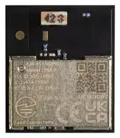
453-00090C
Bluetooth Module, BLE 5.3, 2 Mbps, -96.2 dBm, 1.8 V to 3.8 V, -40 °C to 105 °C
⚠️ Reference pricing provided. In case of supply shortages, we will connect you with our trusted procurement partners to ensure your project's continuity.
- Manufacturer: EZURIO
- Product type: Bluetooth Modules & Adaptors
- SVHC: To Be Advised
- Interfaces: I2C, SPI, USART
- Product Range: Lyra Series
- Certifications: CE, FCC, ISED, KC, MIC
- Bluetooth Class: -
- Bluetooth Version: Bluetooth 5.3
- Supply Voltage Range: 1.8 V to 3.8 V
- Receiver Sensitivity Rx: -96.2 dBm
- Operating Temperature Range: -40 °C to 105 °C
| Delivery and price | |
|---|---|
| Units per pack | 250 |
| Price | 4.65 € |
| Current stock | 25+ |
| Lead time | 30 days |
Datasheet

A

_Version 1.3_

|**Version**|**Date**|**Notes**|**Contributors**|**Approver**|
|---|---|---|---|---|
|1.0|18 Feb 2022|Initial release.|Raj Khatri,<br>Dave Drogowski|Jonathan Kaye|
|1.1|10 June 2022|Updates to5 Reference Diagramsand added<br>5.3 Boot.|Greg Leach,<br>Raj Khatri,<br>Dave Drogowski|Jonathan Kaye|
|1.2|7 Sept 2022|Fixed typo in2 Ordering Information.|Dave Drogowski|Jonathan Kaye|
|||Added new Wireless Xpress SKU information.|||
|1.3|10 Feb 2023|Updated section2 Ordering Informationand|Greg Leach|Jonathan Kaye|
|||5.3 Bootfor Wireless Xpress part (453-00147).|||


https://www.lairdconnect.com/

**Americas** : +1-800-492-2320 **Europe** : +44-1628-858-940 **Hong Kong** : +852-2762-4823

2 © Copyright 2023 Laird Connectivity All Rights Reserved

|1|Introduction .......................................................................................................................................................................... 5|Introduction .......................................................................................................................................................................... 5|
|---|---|---|
||1.1|Key Features .............................................................................................................................................................. 5|
||1.2|Hardware Features .................................................................................................................................................... 6|
||1.3|Firmware Options ....................................................................................................................................................... 6|
|2|Ordering Information ............................................................................................................................................................ 7||
|3|System Overview ................................................................................................................................................................. 8||
||3.1|Block Diagram ............................................................................................................................................................ 8|
||3.2|EFR32BG22 SoC ....................................................................................................................................................... 8|
||3.3|Antenna ...................................................................................................................................................................... 9|
||3.4|Power Supply ............................................................................................................................................................. 9|
|4|Electrical Characteristics ................................................................................................................................................... 10||
||4.1|Absolute Maximum Ratings ...................................................................................................................................... 10|
||4.2|General Operating Conditions .................................................................................................................................. 10|
||4.3|MCU Current Consumption with 3 V Supply ............................................................................................................ 13|
||4.4|Radio Current Consumption with 3 V Supply ........................................................................................................... 14|
||4.5|RF Transmitter General Characteristics for the 2.4 GHz Band ................................................................................ 15|
||4.6|RF Receiver General Characteristics for the 2.4 GHz Band .................................................................................... 15|
||4.7|RF Receiver Characteristics for Bluetooth Low Energy in the 2.4 GHz Band 1 Mbps Data Rate ............................. 16|
||4.8|RF Receiver Characteristics for Bluetooth Low Energy in the 2.4 GHz Band 2 Mbps Data Rate ............................. 17|
||4.9|RF Receiver Characteristics for Bluetooth Low Energy in the 2.4 GHz Band 500 kbps Data Rate .......................... 18|
||4.10|RF Receiver Characteristics for Bluetooth Low Energy in the 2.4 GHz Band 125 kbps Data Rate .......................... 19|
||4.11|High-Frequency Crystal ............................................................................................................................................ 20|
||4.12|Low-Frequency Crystal ............................................................................................................................................ 20|
||4.13|Precision Low Frequency RC Oscillator (LFRCO) ................................................................................................... 20|
||4.14|GPIO Pins ................................................................................................................................................................ 21|
||4.15|Microcontroller Peripherals ....................................................................................................................................... 22|
||4.16|Typical Performance Curves .................................................................................................................................... 23|
|5|Reference Diagrams .......................................................................................................................................................... 24||
||5.1|Network Co-Processor (NCP) Application with UART Host ..................................................................................... 24|
||5.2|SoC Application ........................................................................................................................................................ 25|
||5.3|Boot .......................................................................................................................................................................... 25|
|6|Pin Definitions.................................................................................................................................................................... 26|Pin Definitions.................................................................................................................................................................... 26|
||6.1|Lyra P 31-Pin PCB Module Pinout ........................................................................................................................... 26|
||6.2|Alternate Function Table .......................................................................................................................................... 27|
||6.3|Analog Peripheral Connectivity ................................................................................................................................ 28|
||6.4|Digital Peripheral Connectivity ................................................................................................................................. 29|
|7|Design Guidelines ............................................................................................................................................................. 32||
||7.1|Layout and Placement.............................................................................................................................................. 32|


https://www.lairdconnect.com/

**Americas** : +1-800-492-2320 **Europe** : +44-1628-858-940 **Hong Kong** : +852-2762-4823

3

© Copyright 2023 Laird Connectivity All Rights Reserved

||7.2|Proximity to Other Materials ..................................................................................................................................... 33|
|---|---|---|
||7.3|Proximity to Human Body ......................................................................................................................................... 33|
|8|Mechanical Specifications ................................................................................................................................................. 34||
||8.1|Dimensions .............................................................................................................................................................. 34|
||8.2|PCB Land Pattern .................................................................................................................................................... 35|
||8.3|Lyra P Label Marking ............................................................................................................................................... 36|
|9|Soldering Recommendations ............................................................................................................................................ 37||
||9.1|Reflow for lead Free Solder Paste ........................................................................................................................... 37|
||9.2|Recommended Reflow Profile for lead Free Solder Paste ....................................................................................... 37|
|10|Miscellaneous .................................................................................................................................................................... 38||
||10.1|Cleaning ................................................................................................................................................................... 38|
||10.2|Rework ..................................................................................................................................................................... 38|
||10.3|Handling and Storage............................................................................................................................................... 38|
|11|Tape and Reel ................................................................................................................................................................... 39|Tape and Reel ................................................................................................................................................................... 39|
|12|Regulatory ......................................................................................................................................................................... 40||
|13|Bluetooth SIG Qualification ............................................................................................................................................... 41||
||13.1|Overview .................................................................................................................................................................. 41|
||13.2|Qualification Steps When Referencing on End Product Listing ................................................................................ 41|
|14|Additional Information ........................................................................................................................................................ 43||


https://www.lairdconnect.com/

**Americas** : +1-800-492-2320 **Europe** : +44-1628-858-940 **Hong Kong** : +852-2762-4823

4

© Copyright 2023 Laird Connectivity All Rights Reserved

The Lyra P is a module designed and built to meet the performance, security, and reliability requirements of battery-powered IoT products running on Bluetooth networks.

Based on the EFR32BG22 SoC, the Lyra P enables Bluetooth[® ] Low Energy connectivity while delivering best-in-class RF range and performance, future-proof capability for feature and OTA firmware updates, enhanced security features, and low energy consumption.

Lyra P modules are a full solution that comes with fully upgradeable, robust software stacks, world-wide regulatory certifications, advanced development and debugging tools, and support that will minimize and simplify the engineering and development of your end-products helping to accelerate their time-to-market.

The Lyra P is intended for a broad range of applications, including:

- Asset Tags and Beacons

- Sports, Fitness, and Wellness devices

- Portable Medical

- Connected Home

- Industrial and Building Automation

- Bluetooth mesh Low Power Node

- Bluetooth 5.3

- Bluetooth mesh Low Power Node

- Built-in antenna

- Up to 8 dBm TX power

   - 32-bit ARM Cortex-M33 core at up to 76.8 MHz

   - 512/32 kB of Flash/RAM memory

   - Optimal selection of MCU peripherals

   - Up to 24 GPIO pins

- -98.9 dBm BLE RX sensitivity at 1 Mbps ▪ 12.9 mm x 15.0 mm

https://www.lairdconnect.com/

**Americas** : +1-800-492-2320 **Europe** : +44-1628-858-940 **Hong Kong** : +852-2762-4823

5 © Copyright 2023 Laird Connectivity All Rights Reserved

## • **Supported Protocols**

- Bluetooth Low Energy (Bluetooth 5.3)

   - Direction finding

   - 1M, 2M and LE Coded PHYs

- Bluetooth Mesh Low Power Node

## • **Wireless System-on-Chip**

- 2.4 GHz radio

- TX power up to +8 dBm

- High-performance 32-bit ARM Cortex-M33® with DSP instruction and floating-point unit for efficient signal processing

- 512 kB flash program memory

- 32 kB RAM data memory

- Embedded Trace Macrocell (ETM) for advanced debugging

## • **High-Receiver Performance**

- -106.7 dBm sensitivity (0.1% BER) at 125 kbps GFSK

- -102.5 dBm sensitivity (0.1% BER) at 500 kbps GFSK

- -98.9 dBm sensitivity (0.1% BER) at 1 Mbps GFSK

- -96.2 dBm sensitivity (0.1% BER) at 2 Mbps GFSK

## • **Low-Energy Consumption**

   - 4.3 mA RX current at 1 Mbps GFSK

   - 4.8 mA TX current at 0 dBm output power

   - 10.6 mA TX current at 8 dBm output power

   - 26 µA/MHz in Active Mode (EM0)

   - 1.40 μA EM2 DeepSleep current (RTCC running from LFXO, Full RAM retention)

- **Regulatory Certifications**

   - FCC

   - CE

   - ISED

   - MIC/TELEC

   - KCC

## • **Wide Operating Range**

   - 1.8 to 3.8 V

   - -40 to +105°C

- **Dimensions**

   - 12.9 mm x 15.0 mm x 2.2 mm

- **Security Features**

   - Secure Boot with Root of Trust and Secure Loader (RTSL)

   - Hardware Cryptographic Acceleration for AES128/256, SHA-1, SHA-2 (up to 256-bit), ECC (up to 256-bit), ECDSA, and ECDH

   - True Random Number Generator (TRNG) compliant with NIST SP800-90 and AIS-31

   - ARM® TrustZone®

   - Secure Debug with lock/unlock

- **Wide Selection of MCU Peripherals**

   - Analog to Digital Converter (ADC)

      - 12-bit @ 1 Msps

      - 16-bit @ 76.9 ksps

   - Up to 24 General Purpose I/O pins with output state retention and asynchronous interrupts

   - 8 Channel DMA Controller

   - 12 Channel Peripheral Reflex System (PRS)

   - 4 × 16-bit Timer/Counter with 3 Compare/Capture/PWM channels

   - 1 × 32-bit Timer/Counter with 3 Compare/Capture/PWM channels

   - 32-bit Real Time Counter

   - 24-bit Low Energy Timer for waveform generation

   - 1 × Watchdog Timer

   - 2 × Universal Synchronous/Asynchronous Receiver/Transmitter (UART/SPI/SmartCard (ISO 7816)/IrDA/I2S)

   - 1 × Enhanced Universal Asynchronous Receiver/Transmitter (EUART)

   - 2 × I2C interface with SMBus support

   - Digital microphone interface (PDM)

   - RFSENSE with selective OOK mode

The Lyra series supports three different firmware options for software development:

**AT Command Set –** fully featured and extensible to suit any developer’s needs.

- Proven over 5+ years

- Basic Bluetooth LE cable replacement

- Simplest implementation possible

- ▪ Includes all key features of Wireless Xpress and more

**Wireless Xpress –** Frozen at current release, path for existing Silicon Labs customers

- Basic Bluetooth LE cable replacement

- Secure FOTA capable FW

- Xpress command API for iOS & Android

**C Code –** Full software development with Silicon Labs SDK and Toolchain

- Native C code development

- Use Simplicity Studio IDE

- Full functionality of Silicon Labs HW / SW

https://www.lairdconnect.com/

**Americas** : +1-800-492-2320 **Europe** : +44-1628-858-940 **Hong Kong** : +852-2762-4823

6

© Copyright 2023 Laird Connectivity All Rights Reserved

## _**Table 1: Ordering Information**_

|**Part**|**Description**|
|---|---|
|453-00090R|Lyra Series - Bluetooth v5.3 PCB Module with integrated antenna (Silicon Labs EFR32BG22) - Tape / Reel|
|453-00090C|Lyra Series - Bluetooth v5.3 PCB Module with integrated antenna (Silicon Labs EFR32BG22) – Cut / Tape|
|453-00147R|Lyra Series - Bluetooth v5.3 PCB Module, Integrated Antenna, Wireless Xpress FW (Silicon Labs|
||EFR32BG22) - Tape / Reel|
|453-00147C|Lyra Series - Bluetooth v5.3 PCB Module, Integrated Antenna, Wireless Xpress FW (Silicon Labs|
||EFR32BG22) – Cut / Tape|
|453-00090-K1|Lyra Series - Development Kit - Bluetooth v5.3 PCB Module with integrated antenna|


**Note** : Part 453-00147 ships from the factory configured with Laird Connectivity’s Organizational Unique Identifier (OUI) (18-C2-93) in One Time Programmable memory. This is used as the basis for the part Bluetooth address.

Legacy BGX220P parts shipped with Silabs’ OUI (60-A4-23).

https://www.lairdconnect.com/

**Americas** : +1-800-492-2320 **Europe** : +44-1628-858-940 **Hong Kong** : +852-2762-4823

7 © Copyright 2023 Laird Connectivity All Rights Reserved

The Lyra P module combines an energy-friendly MCU with a highly integrated radio transceiver in a PCB module with a robust, integrated antenna. This section gives a short introduction to the features of the module.

_**Figure 1: Lyra P Block Diagram**_

The block diagram for the Lyra P module is shown in Figure 1. The wireless module includes the EFR32BG22 wireless System on a Chip (SoC), required decoupling capacitors and inductors, 38.4 MHz and 32.768 kHz crystals, RF matching circuit, and integrated chip antenna.

A simplified internal schematic for the Lyra P module is shown in Figure 2.

_**Figure 2: Lyra P Module Schematic**_

## $3.2 EFRS2BG22 SoC

The EFR32BG22 SoC features a 32-bit ARM Cortex M33 core, a 2.4 GHz high-performance radio, 512 kB of flash memory, a rich set of MCU peripherals, and various clock management and serial interfacing options. Consult the EFR32xG22 Wireless Gecko Reference Manual and the EFR32BG22 Data Sheet for details.

https://www.lairdconnect.com/

8 **Americas** : +1-800-492-2320 © Copyright 2023 Laird Connectivity **Europe** : +44-1628-858-940 All Rights Reserved **Hong Kong** : +852-2762-4823

## 3.5 Antenna

Lyra P modules include a ceramic chip antenna on board with the characteristics detailed in the table below.

_**Table 2: Antenna Efficiency and Peak Gain**_

||**With**||
|---|---|---|
|**Parameter**|**optimal**|**Note**|
||**layout**||
|Efficiency|-1 dB|Antenna efficiency, gain and radiation pattern are highly dependent on the application PCB|
|Peak gain|1.86 dBi|layout and mechanical design. Refer toDesign Guidelines for recommendations to achieve<br>optimal antenna performance.|


## 3.4 Power Supply

The Lyra P requires a single nominal supply level of 3.0 V to operate. All necessary decoupling and filtering components are included in the module.

https://www.lairdconnect.com/

**Americas** : +1-800-492-2320 **Europe** : +44-1628-858-940 **Hong Kong** : +852-2762-4823

9 © Copyright 2023 Laird Connectivity All Rights Reserved

All electrical parameters in all tables are specified under the following conditions, unless stated otherwise:

- Typical values are based on TA=25 °C and VDD supply at 3.0 V, by production test and/or technology characterization.

- Radio performance numbers are measured in conducted mode, based on Silicon Laboratories reference designs using output power-specific external RF impedance-matching networks for interfacing to a 50 Ω antenna.

- Minimum and maximum values represent the worst conditions across supply voltage, process variation, and operating temperature, unless stated otherwise.

Stresses beyond those listed below may cause permanent damage to the device. This is a stress rating only and functional operation of the devices at those or any other conditions beyond those indicated in the operation listings of this specification is not implied. Exposure to maximum rating conditions for extended periods may affect device reliability.

_**Table 3: Absolute Maximum Ratings**_

|**_Table 3: Absolute Maximum Ratings_**|||||||
|---|---|---|---|---|---|---|
|**Parameter**|**Symbol**|**Test Condition**|**Min**|**Typ**|**Max**|**Unit**|
|Storage temperature range|TSTG||-40|—|+105|°C|
|Voltage on VDD supply pin|VDDMAX||-0.3|—|3.8|V|
|Voltage ramp rate on VDD supply pin|VDDRAMPMAX||—|—|1.0|V / µs|
|DC voltage on any GPIO pin|VDIGPIN||-0.3|—|VVDD+ 0.3|V|
|Total current into VDD pin|IVDDMAX|Source|—|—|200|mA|
|Total current into GND pin|IGNDMAX|Sink|—|—|200|mA|
|Current per I/O pin|IIOMAX|Sink|—|—|50|mA|
|||Source|—|—|50|mA|
|Current for all I/O pins|IIOALLMAX|Sink|—|—|200|mA|
|||Source|—|—|200|mA|


## 4.2 General Operating Conditions

This table specifies the general operating temperature range and supply voltage range for all supplies. The minimum and maximum values of all other tables are specified over this operating range, unless otherwise noted.

|**Parameter**|**Symbol**|**Test Condition**|**Min**|**Typ**|**Max**|**Unit**|
|---|---|---|---|---|---|---|
|Operating ambient|TA|-G temperature grade|-40|—|+85|°C|
|temperature range||-N temperature grade|-40|—|+105|°C|
|VDD operating supply|VVDD|DCDC in regulation1|2.2|3.0|3.8|V|
|voltage|||||||
|||DCDC in bypass|1.8|3.0|3.8|V|
|HCLK and SYSCLK frequency|fHCLK|VSCALE2, MODE =|—|—|76.8|MHz|
|||WS1|||||
|||VSCALE2, MODE =|—|—|40|MHz|
|||WS0|||||
|||VSCALE1, MODE =|—|—|40|MHz|
|||WS0|||||


https://www.lairdconnect.com/

**Americas** : +1-800-492-2320 **Europe** : +44-1628-858-940 **Hong Kong** : +852-2762-4823

10

© Copyright 2023 Laird Connectivity All Rights Reserved

|**Parameter**|**Symbol**|**Test Condition**|**Min**|**Typ**|**Max**|**Unit**|
|---|---|---|---|---|---|---|
|PCLK frequency|fPCLK|VSCALE2|—|—|50|MHz|
|||VSCALE1|—|—|40|MHz|
|EM01 Group A clock|fEM01GRPACLK|VSCALE2|—|—|76.8|MHz|
|frequency||VSCALE1|—|—|40|MHz|
|EM01 Group B clock|fEM01GRPBCLK|VSCALE2|—|—|76.8|MHz|
|frequency||VSCALE1|—|—|40|MHz|
|Radio HCLK frequency|fRHCLK|VSCALE2 or|—|38.4|—|MHz|
|||VSCALE1|||||


## **Note:**

1. The supported maximum VVDD in regulation mode is a function of temperature and 10-year lifetime average load current. See more details in DC-DC Operating Limits.

https://www.lairdconnect.com/

**Americas** : +1-800-492-2320 **Europe** : +44-1628-858-940 **Hong Kong** : +852-2762-4823

11 © Copyright 2023 Laird Connectivity All Rights Reserved

The maximum supported voltage on the VDD supply pin is limited under certain conditions. Maximum input voltage is a function of temperature and the average load current over a 10-year lifetime. Figure 3 shows the safe operating region under specific conditions. Exceeding this safe operating range may impact the reliability and performance of the DC-DC converter.

The average load current for an application can typically be determined by examining the current profile during the time the device is powered. For example, an application that is continuously powered which spends 99% of the time asleep consuming 2 µA and 1% of the time active and consuming 10 mA has an average lifetime load current of about 102 µA.

_**Figure 3: Lifetime average load current limit vs. maximum input voltage**_

The minimum input voltage for the DC-DC in EM0/EM1 mode is a function of the maximum load current, and the peak current setting. Figure 4 shows the max load current vs. input voltage for different DC-DC peak inductor current settings.

_**Figure 4: Transient maximum load current vs. Minimum input voltage**_

https://www.lairdconnect.com/

**Americas** : +1-800-492-2320 **Europe** : +44-1628-858-940 **Hong Kong** : +852-2762-4823

12 © Copyright 2023 Laird Connectivity All Rights Reserved

## 4.5 MCU Current Consumption with 3 V Supply

Unless otherwise indicated, typical conditions are: Module supply voltage = 3.0 V. Voltage scaling level = VSCALE1. TA = 25 °C. Mini mum and maximum values in this table represent the worst conditions across process variation at TA = 25 °C.

_**Table 4: MCU Current Consumption with 3 V Supply**_

|**Parameter**|**Symbol**|**Test Condition**|**Min**|**Typ**|**Max**|**Unit**|
|---|---|---|---|---|---|---|
|Current consumption in EM0|IACTIVE|76.8 MHz HFRCO w/ DPLL referenced to|—|27|—|µA/MHz|
|mode with all peripherals||38.4 MHz crystal, CPU running while loop|||||
|disabled||from flash, VSCALE2|||||
|||76.8 MHz HFRCO w/ DPLL referenced to|—|37|—|µA/MHz|
|||38.4 MHz crystal, CPU running CoreMark|||||
|||loop from flash, VSCALE2|||||
|||38.4 MHz crystal, CPU running Prime|—|28|—|µA/MHz|
|||from flash|||||
|||38.4 MHz crystal, CPU running while loop|—|26|—|µA/MHz|
|||from flash|||||
|||38.4 MHz crystal, CPU running CoreMark|—|38|—|µA/MHz|
|||loop from flash|||||
|||38 MHz HFRCO, CPU running while loop|—|22|—|µA/MHz|
|||from flash|||||
|||76.8 MHz HFRCO w/ DPLL referenced to|—|28|—|µA/MHz|
|||38.4 MHz crystal, CPU running Prime|||||
|||from flash, VSCALE2|||||
|Current consumption in EM1|IEM1|76.8 MHz HFRCO w/ DPLL referenced to|—|17|—|µA/MHz|
|mode with all peripherals||38.4 MHz crystal, VSCALE2|||||
|disabled|||||||
|||38.4 MHz crystal|—|17|—|µA/MHz|
|||38 MHz HFRCO|—|13|—|µA/MHz|
|Current consumption in EM2|IEM2_VS|Full RAM retention and RTC running from|—|1.40|—|µA|
|mode, VSCALE0||LFXO|||||
|||Full RAM retention and RTC running from|—|1.40|—|µA|
|||LFRCO|||||
|||Full RAM retention and RTC running from|—|1.75|—|µA|
|||LFRCO in precision mode|||||
|||24 kB RAM retention and RTC running|—|1.32|—|µA|
|||from LFXO|||||
|||24 kB RAM retention and RTC running|—|1.66|—|µA|
|||from LFRCO in precision mode|||||
|||8 kB RAM retention and RTC running|—|1.21|—|µA|
|||from LFXO|||||


https://www.lairdconnect.com/

**Americas** : +1-800-492-2320 **Europe** : +44-1628-858-940 **Hong Kong** : +852-2762-4823

13 © Copyright 2023 Laird Connectivity All Rights Reserved

|**Parameter**|**Symbol**|**Test Condition**|**Min**|**Typ**|**Max**|**Unit**|
|---|---|---|---|---|---|---|
|||8 kB RAM retention and RTC running|—|1.20|—|µA|
|||from LFRCO|||||
|Current consumption in EM3|IEM3_VS|8 kB RAM retention and RTC running|—|1.05|—|µA|
|mode, VSCALE0||from ULFRCO|||||
|Current consumption in EM4|IEM4|No BURTC, No LF Oscillator, DCDC|—|0.17|—|µA|
|mode||bypassed|||||
|Additional current in EM2 or|IPD0B_VS||—|0.37|—|µA|
|EM3 when any peripheral in|||||||
|PD0B is enabled1|||||||


**Note:** 1. Extra current consumed by power domain. Does not include current associated with the enabled peripherals. See for a list of the peripherals in each power domain.

## 4.4 Radio Current Consumption with 3 V Supply

RF current consumption measured with MCU in EM1, HCLK = 38.4 MHz, and all MCU peripherals disabled. Unless otherwise indicated, typical conditions are: VDD = 3.0 V. TA = 25 °C. Minimum and maximum values in this table represent the worst conditions across process variation at TA = 25 °C.

|Parameter|Symbol|Test Condition|Min|Typ|Max|Unit|
|---|---|---|---|---|---|---|
|System current consumption in receive|IRX_ACTIVE|125 kbit/s, 2GFSK, f = 2.4 GHz,|—|4.5|—|mA|
|mode, active packet reception||Bluetooth stack running|||||
|||500 kbit/s, 2GFSK, f = 2.4 GHz,|—|4.5|—|mA|
|||Bluetooth stack running|||||
|||1 Mbit/s, 2GFSK, f = 2.4 GHz,|—|4.3|—|mA|
|||Bluetooth stack running|||||
|||2 Mbit/s, 2GFSK, f = 2.4 GHz,|—|4.8|—|mA|
|||Bluetooth stack running|||||
|System current consumption in receive|IRX_LISTEN|125 kbit/s, 2GFSK, f = 2.4 GHz,|—|4.4|—|mA|
|mode, listening for packet||Bluetooth stack running|||||
|||500 kbit/s, 2GFSK, f = 2.4 GHz,|—|4.4|—|mA|
|||Bluetooth stack running|||||
|||1 Mbit/s, 2GFSK, f = 2.4 GHz,|—|4.2|—|mA|
|||Bluetooth stack running|||||
|||2 Mbit/s, 2GFSK, f = 2.4 GHz,|—|4.7|—|mA|
|||Bluetooth stack running|||||
|System current consumption in transmit|ITX|f = 2.4 GHz, CW, 0 dBm output|—|4.8|—|mA|
|mode||power|||||
|||f = 2.4 GHz, CW, 6 dBm output|—|8.8|—|mA|
|||power|||||
|||f = 2.4 GHz, CW, 8 dBm output|—|10.6|—|mA|
|||power|||||


https://www.lairdconnect.com/

**Americas** : +1-800-492-2320 **Europe** : +44-1628-858-940 **Hong Kong** : +852-2762-4823

14 © Copyright 2023 Laird Connectivity All Rights Reserved

## 4.5 RF Transmitter General Characteristics for the 2.4 GHz Band

Unless otherwise indicated, typical conditions are: TA = 25 °C, VDD = 3.0V. RF center frequency 2.45 GHz.

|**Parameter**|**Symbol**|**Test Condition**|**Test Condition**(Output<br>Power)|**Min**|**Typ**|**Max**|**Unit**|
|---|---|---|---|---|---|---|---|
|RF tuning frequency range|FRANGE|||2400|—|2483.5|MHz|
|Maximum TX power|POUTMAX|8 dBm|8 dBm|—|8.2|—|dBm|
|Minimum active TX Power|POUTMIN|8 dBm|8 dBm|—|-27|—|dBm|
|Output power variation vs VDD supply|POUTVAR_V|8 dBm with VDD voltage|8 dBm with VDD voltage|—|0.04|—|dB|
|voltage variation, frequency = 2450 MHz||swept from 1.8 V to 3.0 V||||||
|Output power variation vs temperature,|POUTVAR_T|8 dBm, (-40 to +105 °C)||—|0.9|—|dB|
|Frequency = 2450 MHz||||||||
|Output power variation vs RF frequency|POUTVAR_F|8 dBm|8 dBm|—|0.2|—|dB|


## 4.6 RF Receiver General Characteristics for the 2.4 GHz Band

Unless otherwise indicated, typical conditions are: TA = 25 °C, VDD = 3.0V. RF center frequency 2.45 GHz.

**Table 5: RF Receiver General Characteristics for the 2.4 GHz Band**

|**Parameter**|**Symbol**|**Test Condition**|**Min**|**Typ**|**Max**|**Unit**|
|---|---|---|---|---|---|---|
|RF tuning frequency range|FRANGE||2400|—|2483.5|MHz|


https://www.lairdconnect.com/

**Americas** : +1-800-492-2320 **Europe** : +44-1628-858-940 **Hong Kong** : +852-2762-4823

15 © Copyright 2023 Laird Connectivity All Rights Reserved

## 4.7 RF Receiver Characteristics for Bluetooth Low Energy in the 2.4

Unless otherwise indicated, typical conditions are: TA = 25 °C, VDD = 3.0V. RF center frequency 2.45 GHz.

_**Table 6: RF Receiver Characteristics for Bluetooth Low Energy in the 2.4 GHz Band 1 Mbps Data Rate**_

|**Parameter**|**Symbol**||**Test Condition**|**Test Condition**|||**Min**|**Typ**|**Max**|**Unit**|
|---|---|---|---|---|---|---|---|---|---|---|
|Max usable receiver|SAT|Signal is reference signal1|||||—|10|—|dBm|
|input level|||||||||||
|Sensitivity|SENS|Signal is reference signal, 37 byte payload||Signal is reference signal, 37 byte payload2|||—|-|—|dBm|
|||||||||98.9|||
|||Signal is reference signal, 255 byte||Signal is reference signal, 255 byte|Signal is reference signal, 255 byte||—|-|—|dBm|
|||payload1||||||97.4|||
|||With non-ideal signals3 1|||||—|-|—|dBm|
|||||||||96.9|||
|Signal to co-channel|C/ICC|(see notes)1 4|||||—|8.7|—|dB|
|interferer|||||||||||
|N ± 1 Adjacent channel|C/I1|Interferer is reference signal at +1 MHz|Interferer is reference signal at +1 MHz||||—|-6.6|—|dB|
|selectivity||offset1 5 4 6|||||||||
|||Interferer is reference signal at -1 MHz|Interferer is reference signal at -1 MHz||||—|-6.5|—|dB|
|||offset1 5 4 6|||||||||
|N ± 2 Alternate channel|C/I2|Interferer is reference signal at +2 MHz|Interferer is reference signal at +2 MHz||||—|-|—|dB|
|selectivity||offset1 5 4 6||||||40.9|||
|||Interferer is reference signal at -2 MHz|Interferer is reference signal at -2 MHz||||—|-|—|dB|
|||offset1 5 4 6||||||39.9|||
|N ± 3 Alternate channel|C/I3|Interferer is reference signal at +3 MHz|Interferer is reference signal at +3 MHz||||—|-|—|dB|
|selectivity||offset1 5 4 6||||||45.9|||
|||Interferer is reference signal at -3 MHz|Interferer is reference signal at -3 MHz||||—|-|—|dB|
|||offset1 5 4 6||||||46.2|||
|Selectivity to image|C/IIM|Interferer is reference signal at image|Interferer is reference signal at image||||—|-|—|dB|
|frequency||frequencywith 1 MHzprecision1 6||||||23.5|||
|Selectivity to image|C/IIM_1|Interferer is reference signal at image|Interferer is reference signal at image||||—|-|—|dB|
|frequency ± 1 MHz||frequency +1 MHz with 1||||||40.9|||
|||MHz precision1 6|||||||||
|||Interferer|is<br>reference|signal|at|image|—|-6.6|—|dB|
|||frequency-1 MHz with 1 MHzprecision1 6||||1 6|||||
|Intermodulation|IM|n = 3 (see note7)|||||—|-|—|dBm|
|performance||||||||17.1|||
|**Note:**|||||||||||


1. 0.017% Bit Error Rate.

2. 0.1% Bit Error Rate.

3. With non-ideal signals as specified in Bluetooth Test Specification RF-PHY.TS.5.0.1 section 4.7.1

4. Desired signal -67 dBm.

5. Desired frequency 2402 MHz ≤ Fc ≤ 2480 MHz. 6. With allowed exceptions. 7. As specified in Bluetooth Core specification version 5.1, Vol 6, Part A, Section 4.4

https://www.lairdconnect.com/

**Americas** : +1-800-492-2320 **Europe** : +44-1628-858-940 **Hong Kong** : +852-2762-4823

16 © Copyright 2023 Laird Connectivity All Rights Reserved

## 4.8 RF Receiver Characteristics for Bluetooth Low Energy in the 2.4

Unless otherwise indicated, typical conditions are: TA = 25 °C, VDD = 3.0V. RF center frequency 2.45 GHz.

**Table 7: RF Receiver Characteristics for Bluetooth Low Energy in the 2.4 GHz Band 2 Mbps Data Rate**

|**Parameter**|**Symbol**||**Test Condition**|**Test Condition**|||**Min**|**Typ**|**Max**|**Unit**|
|---|---|---|---|---|---|---|---|---|---|---|
|Max usable receiver|SAT|Signal is reference signal1|||||—|10|—|dBm|
|input level|||||||||||
|Sensitivity|SENS|Signal is reference signal, 37 byte payload||Signal is reference signal, 37 byte payload2|||—|-|—|dBm|
|||||||||96.2|||
|||Signal is reference signal, 255 byte||Signal is reference signal, 255 byte|Signal is reference signal, 255 byte||—|-|—|dBm|
|||payload1||||||94.6|||
|||With non-ideal signals3 1|||||—|-|—|dBm|
|||||||||94.4|||
|Signal to co-channel|C/ICC|(see notes)1 4|||||—|8.8|—|dB|
|interferer|||||||||||
|N ± 1 Adjacent channel|C/I1|Interferer is reference signal at +2 MHz|Interferer is reference signal at +2 MHz||||—|-9.2|—|dB|
|selectivity||offset1 5 4 6|||||||||
|||Interferer is reference signal at -2 MHz|Interferer is reference signal at -2 MHz||||—|-6.6|—|dB|
|||offset1 5 4 6|||||||||
|N ± 2 Alternate channel|C/I2|Interferer is reference signal at +4 MHz|Interferer is reference signal at +4 MHz||||—|-|—|dB|
|selectivity||offset1 5 4 6||||||43.3|||
|||Interferer is reference signal at -4 MHz|Interferer is reference signal at -4 MHz||||—|-|—|dB|
|||offset1 5 4 6||||||44.0|||
|N ± 3 Alternate channel|C/I3|Interferer is reference signal at +6 MHz|Interferer is reference signal at +6 MHz||||—|-|—|dB|
|selectivity||offset1 5 4 6||||||48.6|||
|||Interferer is reference signal at -6 MHz|Interferer is reference signal at -6 MHz||||—|-|—|dB|
|||offset1 5 4 6||||||50.7|||
|Selectivity to image|C/IIM|Interferer is reference signal at image|Interferer is reference signal at image||||—|-|—|dB|
|frequency||frequencywith 1 MHzprecision1 6||||||23.8|||
|Selectivity to image|C/IIM_1|Interferer is reference signal at image|Interferer is reference signal at image||||—|-|—|dB|
|frequency ± 2 MHz||frequency +2 MHz with 1||||||43.3|||
|||MHz precision1 6|||||||||
|||Interferer|is<br>reference|signal|at|image|—|-9.2|—|dB|
|||frequency-2 MHz with 1 MHzprecision1 6||||1 6|||||
|Intermodulation|IM|n = 3 (see note7)|||||—|-|—|dBm|
|performance||||||||18.8|||
|**Note:**|||||||||||


1. 0.017% Bit Error Rate.

2. 0.1% Bit Error Rate.

3. With non-ideal signals as specified in Bluetooth Test Specification RF-PHY.TS.5.0.1 section 4.7.1

4. Desired signal -64 dBm.

5. Desired frequency 2402 MHz ≤ Fc ≤ 2480 MHz.

6. With allowed exceptions.

7. As specified in Bluetooth Core specification version 5.1, Vol 6, Part A, Section 4.4

https://www.lairdconnect.com/

**Americas** : +1-800-492-2320 **Europe** : +44-1628-858-940 **Hong Kong** : +852-2762-4823

17 © Copyright 2023 Laird Connectivity All Rights Reserved

## 4.9 RF Receiver Characteristics for Bluetooth Low Energy in the 2.4

Unless otherwise indicated, typical conditions are: TA = 25 °C, VDD = 3.0V. RF center frequency 2.45 GHz.

_**Table 8: RF Receiver Characteristics for Bluetooth Low Energy in the 2.4 GHz Band 500 kbps Data Rate**_

|**Parameter**|**Symbol**|**Test Condition**|**Min**|**Typ**|**Max**|**Unit**|
|---|---|---|---|---|---|---|
|Max usable receiver|SAT|Signal is reference signal1|—|10|—|dBm|
|input level|||||||
|Sensitivity|SENS|Signal is reference signal, 37 byte payload2|—|-|—|dBm|
|||||102.5|||
|||Signal is reference signal, 255 byte|—|-|—|dBm|
|||payload1||101.2|||
|||With non-ideal signals3 1|—|-|—|dBm|
|||||100.2|||
|Signal to co-channel|C/ICC|(see notes)1 4|—|2.7|—|dB|
|interferer|||||||
|N ± 1 Adjacent|C/I1|Interferer is reference signal at +1 MHz|—|-8.0|—|dB|
|channel selectivity||offset1 5 4 6|||||
|||Interferer is reference signal at -1 MHz|—|-7.9|—|dB|
|||offset1 5 4 6|||||
|N ± 2 Alternate|C/I2|Interferer is reference signal at +2 MHz|—|-46.5|—|dB|
|channel selectivity||offset1 5 4 6|||||
|||Interferer is reference signal at -2 MHz|—|-49.9|—|dB|
|||offset1 5 4 6|||||
|N ± 3 Alternate|C/I3|Interferer is reference signal at +3 MHz|—|-48.9|—|dB|
|channel selectivity||offset1 5 4 6|||||
|||Interferer is reference signal at -3 MHz|—|-53.8|—|dB|
|||offset1 5 4 6|||||
|Selectivity to image|C/IIM|Interferer is reference signal at image|—|-48.3|—|dB|
|frequency||frequencywith 1 MHzprecision1 6|||||
|Selectivity to image|C/IIM_1|Interferer is reference signal at image|—|-49.9|—|dB|
|frequency ± 1 MHz||frequency +1 MHz with 1|||||
|||MHz precision1 6|||||
|||Interferer is reference signal at image|—|-46.5|—|dB|
|||frequency-1 MHz with 1 MHzprecision1 6|||||


## **Note:**

1. 0.017% Bit Error Rate.

2. 0.1% Bit Error Rate.

3. With non-ideal signals as specified in Bluetooth Test Specification RF-PHY.TS.5.0.1 section 4.7.1

4. Desired signal -72 dBm.

5. Desired frequency 2402 MHz ≤ Fc ≤ 2480 MHz.

6. With allowed exceptions.

https://www.lairdconnect.com/

**Americas** : +1-800-492-2320 **Europe** : +44-1628-858-940 **Hong Kong** : +852-2762-4823

18 © Copyright 2023 Laird Connectivity All Rights Reserved

## 4.10 RF Receiver Characteristics for Bluetooth Low Energy in the 2.4

Unless otherwise indicated, typical conditions are: TA = 25 °C, VDD = 3.0V. RF center frequency 2.45 GHz.

_**Table 9: RF Receiver Characteristics for Bluetooth Low Energy in the 2.4 GHz Band 125 kbps Data Rate**_

|**Parameter**|**Symbol**|**Test Condition**|**Min**|**Typ**|**Max**|**Unit**|
|---|---|---|---|---|---|---|
|Max usable receiver|SAT|Signal is reference signal1|—|10|—|dBm|
|input level|||||||
|Sensitivity|SENS|Signal is reference signal,37 bytepayload2|—|-106.7|—|dBm|
|||Signal is reference signal, 255 byte|—|-106.4|—|dBm|
|||payload1|||||
|||With non-ideal signals3 1|—|-105.8|—|dBm|
|Signal to co-channel|C/ICC|(see notes)1 4|—|0.9|—|dB|
|interferer|||||||
|N ± 1 Adjacent|C/I1|Interferer is reference signal at +1 MHz|—|-13.6|—|dB|
|channel selectivity||offset1 5 4 6|||||
|||Interferer is reference signal at -1 MHz|—|-13.4|—|dB|
|||offset1 5 4 6|||||
|N ± 2 Alternate|C/I2|Interferer is reference signal at +2 MHz|—|-52.6|—|dB|
|channel selectivity||offset1 5 4 6|||||
|||Interferer is reference signal at -2 MHz|—|-55.8|—|dB|
|||offset1 5 4 6|||||
|N ± 3 Alternate|C/I3|Interferer is reference signal at +3 MHz|—|-53.7|—|dB|
|channel selectivity||offset1 5 4 6|||||
|||Interferer is reference signal at -3 MHz|—|-59.0|—|dB|
|||offset1 5 4 6|||||
|Selectivity to image|C/IIM|Interferer is reference signal at image|—|-52.7|—|dB|
|frequency||frequencywith 1 MHzprecision1 6|||||
|Selectivity to image|C/IIM_1|Interferer is reference signal at image|—|-53.7|—|dB|
|frequency ± 1 MHz||frequency +1 MHz with 1|||||
|||MHz precision1 6|||||
|||Interferer is reference signal at image|—|-52.6|—|dB|
|||frequency-1 MHz with 1 MHzprecision1 6|||||


## **Note:**

1. 0.017% Bit Error Rate.

2. 0.1% Bit Error Rate.

3. With non-ideal signals as specified in Bluetooth Test Specification RF-PHY.TS.5.0.1 section 4.7.1

4. Desired signal -79 dBm.

5. Desired frequency 2402 MHz ≤ Fc ≤ 2480 MHz.

6. With allowed exceptions.

https://www.lairdconnect.com/

**Americas** : +1-800-492-2320 **Europe** : +44-1628-858-940 **Hong Kong** : +852-2762-4823

19 © Copyright 2023 Laird Connectivity All Rights Reserved

## 4.11 High-Frequency Crystal

_**Table 10: High-Frequency Crystal**_

|**Parameter**|**Symbol**|**Test Condition**|**Min**|**Typ**|**Max**|**Unit**|
|---|---|---|---|---|---|---|
|Crystal frequency|fHFXTAL||—|38.4|—|MHz|
|Initial calibrated|ACCHFXTAL||-10|±5|10|ppm|
|accuracy|||||||
|Temperature drift|DRIFTHFXTAL|Across specified|-20|—|20|ppm|
|||temperature range|||||


## 4.12 Low-Frequency Crystal

_**Table 11: Low-Frequency Crystal**_

|**Parameter**|**Symbol**|**Test Condition**|**Min**|**Typ**|**Max**|**Unit**|
|---|---|---|---|---|---|---|
|Crystal frequency1|fLFXTAL||—|32.768|—|kHz|
|Temperature drift|DRIFTLFXTAL|-40°C to +85°C|-100|—|100|ppm|
|||-40°C to +105°C|-150|—|150|ppm|


## **Note:**

1. Nominal frequency tolerance of the crystal is ± 20 ppm.

## 4.13 Precision Low Frequency RC Oscillator (LFRCO)

**Table 12: Precision Low Frequency RC Oscillator (LFRCO)**

|**Parameter**|**Symbol**|**Test Condition**|**Min**|**Typ**|**Max**|**Unit**|
|---|---|---|---|---|---|---|
|Nominal oscillation|FLFRCO||—|32.768|—|kHz|
|frequency|||||||
|Frequency accuracy|FLFRCO_ACC|Normal mode|-3|—|3|%|
|||Precision mode1, across|-500|—|500|ppm|
|||operating temperature|||||
|||range2|||||
|Startup time|tSTARTUP|Normal mode|—|204|—|µs|
|||Precision mode1|—|11.7|—|ms|
|Current consumption|ILFRCO|Normal mode|—|175|—|nA|
|||Precision mode1, T = stable|—|655|—|nA|
|||at 25|||||
|||°C3|||||


## **Note:**

1. The LFRCO operates in high-precision mode when CFG_HIGHPRECEN is set to 1. High-precision mode is not available in EM4.

2. Includes ± 40 ppm frequency tolerance of the HFXO crystal.

3. Includes periodic re-calibration against HFXO crystal oscillator.

https://www.lairdconnect.com/

**Americas** : +1-800-492-2320 **Europe** : +44-1628-858-940 **Hong Kong** : +852-2762-4823

20 © Copyright 2023 Laird Connectivity All Rights Reserved

## 4.14GPIO Pins

Unless otherwise indicated, typical conditions are: VDD = 3.0 V.

_**Table 13: GPIO Pins**_

||**Parameter**|**Symbol**|**Test Condition**|**Min**|**Typ**|**Max**|**Unit**|
|---|---|---|---|---|---|---|---|
|Leakage current||ILEAK_IO|MODEx = DISABLED, VDD|—|2.5|—|nA|
||||= 3.0 V|||||
|Input low voltage1||VIL|Any GPIO pin|—|—|0.3 *|V|
|||||||VDD||
||||RESETn|—|—|0.3 *|V|
|||||||DVDD||
|Input high voltage1||VIH|Any GPIO pin|0.7 * VDD|—|—|V|
||||RESETn|0.7 * DVDD|—|—|V|
|Hysteresis of input||VHYS|Any GPIO pin|0.05*VDD|—|—|V|
|voltage|||RESETn|0.05*DVDD|—|—|V|
|Output low voltage||VOL|Sinking 20mA, VDD = 3.0 V|—|—|0.2 *|V|
|||||||VDD||
||||Sinking 8mA, VDD = 1.62 V|—|—|0.4 *|V|
|||||||VDD||
|Output high voltage||VOH|Sourcing 20mA, VDD = 3.0 V|0.8 * VDD|—|—|V|
||||Sourcing 8mA, VDD = 1.62 V|0.6 * VDD|—|—|V|
|GPIO rise time|GPIO rise time|TGPIO_RISE|VDD = 3.0V, Cload= 50pF,|—|8.4|—|ns|
||||SLEWRATE = 4, 10% to|||||
||||90%|||||
||||VDD = 1.7V, Cload= 50pF,|—|13|—|ns|
||||SLEWRATE = 4, 10% to|||||
||||90%|||||
|GPIO fall time|GPIO fall time|TGPIO_FALL|VDD = 3.0V, Cload= 50pF,|—|7.1|—|ns|
||||SLEWRATE = 4, 90% to|||||
||||10%|||||
||||VDD = 1.7V, Cload= 50pF,|—|11.9|—|ns|
||||SLEWRATE = 4, 90% to|||||
||||10%|||||
|Pull up/down||RPULL|GPIO pull-up to VDD:|35|44|55|kΩ|
|resistance|||MODEn = DISABLE,|||||
||||DOUT=1. GPIO pull-|||||
||||down to VSS: MODEn =|||||
||||WIREDORPULLDOWN,|||||
||||DOUT = 0.|||||
||||RESETn pin pull-up to DVDD.|||||
|Maximum filtered glitch||TGF|MODE = INPUT, DOUT = 1|—|27|—|ns|
|width||||||||
|**Note:**|**Note:**|||||||


1. GPIO input thresholds are proportional to the VDD pin. RESETn input thresholds are proportional to the internal DVDD supply, which is generated by the DC-DC converter. DVDD is equal to 1.8 V when DC-DC is active and bypassed to VDD when DC-DC is inactive.

https://www.lairdconnect.com/

**Americas** : +1-800-492-2320 **Europe** : +44-1628-858-940 **Hong Kong** : +852-2762-4823

21 © Copyright 2023 Laird Connectivity All Rights Reserved

## 4.15 Microcontroller Peripherals

The MCU peripherals set available in Lyra P modules includes:

- ADC: 12-bit at 1 Msps, 16-bit at 76.9 ksps

- 16-bit and 32-bit Timers/Counters

- 24-bit Low Energy Timer for waveform generation

- 32-bit Real Time Counter

- USART (UART/SPI/SmartCards/IrDA/I2S)

- EUART (UART/IrDA)

- I[2] C peripheral interfaces

- PDM interface

- 12 Channel Peripheral Reflex System

For details on their electrical performance, consult the relevant portions of Section 4 in the SoC datasheet.

To learn which GPIO ports provide access to every peripheral, consult Analog Peripheral Connectivity and Digital Peripheral Connectivity.

https://www.lairdconnect.com/

**Americas** : +1-800-492-2320 **Europe** : +44-1628-858-940 **Hong Kong** : +852-2762-4823

22 © Copyright 2023 Laird Connectivity All Rights Reserved

## 4.16Typical Performance Curves

Typical performance curves indicate typical characterized performance under the stated conditions.

## 4.16.1 Antenna Radiation and Efficiency

Typical Lyra P radiation patterns and efficiency for the on-board chip antenna under optimal operating conditions are plotted in the figures that follow. Antenna gain and radiation patterns have a strong dependence on the size and shape of the application PCB the module is mounted on, as well as on the proximity of any mechanical design to the antenna.

_**Phi 0[o]**_

_**Phi 90[o]**_

_**Theta 90[o] Radiation Efficiency vs Application Board GND Plane Width**_

_**Figure 5: Typical 2D Antenna Radiation Patterns and Efficiency**_

https://www.lairdconnect.com/

**Americas** : +1-800-492-2320 **Europe** : +44-1628-858-940 **Hong Kong** : +852-2762-4823

23 © Copyright 2023 Laird Connectivity All Rights Reserved

The Lyra P can be controlled over the UART interface as a peripheral to an external host processor. Typical power supply, programming/debug interface, and host interface connections are shown in the figure below.

**Note** : For boot pin, see section 5.3 Boot.

_**Figure 6: UART NCP Configuration**_

https://www.lairdconnect.com/

**Americas** : +1-800-492-2320 **Europe** : +44-1628-858-940 **Hong Kong** : +852-2762-4823

24 © Copyright 2023 Laird Connectivity All Rights Reserved

The Lyra P can be used in a stand-alone SoC configuration without an external host processor. Typical power supply and programming/debug interface connections are shown in the figure below.

_**Figure 7: Stand-Alone SoC Configuration**_

## 5.3 Boot

The BOOT pin is used to determine when execution of the bootloader is required. Upon reset, execution of the bootloader begins. The state of the BOOT pin is read immediately upon start-up of the bootloader. If LOW, execution of the bootloader continues, facilitating firmware update via the UART. If the BOOT pin is HIGH, the bootloader will stop execution and pass control to the main application firmware.

**Note** : To maintain backwards compatibility with legacy BGX220P Wireless Xpress parts, the BOOT pin for 453-00147 is mapped to the legacy part BOOT pin location. Refer to the table below for details of the appropriate part BOOT pin location.

_**Table 14: Different BOOT Pin Locations for Lyra P**_

|||**BOOT Pin Location**|**BOOT Pin Location**|**BOOT Pin Location**|**BOOT Pin Location**|
|---|---|---|---|---|---|
|**Part**||||||
||**Pin Number**|**Pin Number**|||**Pin Description**|
|453-00090||29|||PC07|
|453-00147||19|||PD02|


https://www.lairdconnect.com/

**Americas** : +1-800-492-2320 **Europe** : +44-1628-858-940 **Hong Kong** : +852-2762-4823

25 © Copyright 2023 Laird Connectivity All Rights Reserved

_**Figure 8:  Lyra P 31-Pin PCB Module With LF Crystal Device Pinout**_

The following table provides package pin connections and general descriptions of pin functionality. For detailed information on the supported features for each GPIO pin, see Table 15: GPIO alternate function table, Analog Peripheral Connectivity, and Digital Peripheral Connectivity.

|**Pin**<br>**Name**|**Pin(s)**|**Description**|**Pin**<br>**Name**|**Pin(s)**||**Description**|
|---|---|---|---|---|---|---|
|GND|1|Ground|PB04|2|GPIO||
|PB03|3|GPIO|PB02|4|GPIO||
|PB01|5|GPIO|PB00|6|GPIO||
|PA00|7|GPIO|PA01|8|GPIO||
|PA02|9|GPIO|PA03|10|GPIO||
|PA04|11|GPIO|GND|12|Ground||
|VDD|13|Power|PA05|14|GPIO||
|||supply|||||
|PA06|15|GPIO|PA07|16|GPIO||
|PA08|17|GPIO|PD03|18|GPIO||
|PD02|19|GPIO|GND|20|Ground||
|NC|21|Do not|PC00|22|GPIO||
|||connect|||||
|PC01|23|GPIO|PC02|24|GPIO||
|PC03|25|GPIO|PC04|26|GPIO||
|PC05|27|GPIO|PC06|28|GPIO||


https://www.lairdconnect.com/

26 **Americas** : +1-800-492-2320 © Copyright 2023 Laird Connectivity **Europe** : +44-1628-858-940 All Rights Reserved **Hong Kong** : +852-2762-4823

|**Pin**<br>**Name**|**Pin(s)**|**Description**|**Pin**<br>**Name**|**Pin(s)**|**Description**|
|---|---|---|---|---|---|
||||||Reset Pin. The RESETn pin is pulled up to an internal DVDD|
||||||supply. An external pull-up is not recommended. To apply an|
||||||external reset source to this pin, it is required to only drive|
||||||this pin low during reset, and let the internal pull-up ensure|
|PC07|29|GPIO|RESETn|30|that reset is released. The RESETn pin can be left|
||||||unconnected if no external reset switch or source is used.|
|GND|31|Ground||||


## 6.2 Alternate Function Table

A wide selection of alternate functionality is available for multiplexing to various pins. The following table shows what functions are available on each device pin.

_**Table 15: GPIO alternate function table**_

|**GPIO**||**Alternate Function**|**Alternate Function**|
|---|---|---|---|
|PB03|GPIO.EM4WU4|GPIO.EM4WU4||
|PB01|GPIO.EM4WU3|GPIO.EM4WU3||
|PB00|IADC0.VREFN|||
|PA00|IADC0.VREFP|||
|PA01|GPIO.SWCLK|||
|PA02|GPIO.SWDIO|||
|PA03|GPIO.SWV|GPIO.TDO|GPIO.TRACEDATA0|
|PA04|GPIO.TDI|GPIO.TRACECLK||
|PA05|GPIO.EM4WU0|GPIO.EM4WU0||
|PD02|GPIO.EM4WU9|GPIO.EM4WU9||
|PC00|GPIO.EM4WU6|GPIO.EM4WU6<br>GPIO.THMSW_EN|GPIO.THMSW_EN|
|PC05|GPIO.EM4WU7|GPIO.EM4WU7||
|PC07|GPIO.EM4WU8|GPIO.EM4WU8||


https://www.lairdconnect.com/

**Americas** : +1-800-492-2320 **Europe** : +44-1628-858-940 **Hong Kong** : +852-2762-4823

27 © Copyright 2023 Laird Connectivity All Rights Reserved

## 6.3 Analog Peripheral Connectivity

Many analog resources are routable and can be connected to numerous GPIO's. The table below indicates which peripherals are available on each GPIO port. When a differential connection is being used, positive inputs are restricted to the EVEN pins and Negative inputs are restricted to the ODD pins. When a single ended connection is being used positive input is available on all pins. See the SoC Reference Manual for more details on the ABUS and analog peripherals.

_**Table 16: ABUS Routing Table**_

|**Peripheral**||**Signal**|**EVEN**|**PA**<br>**ODD**|**PA**<br>**ODD**|**EVEN**|**PB**<br>**ODD**|**PB**<br>**ODD**|**EVEN**|**PC**<br>**ODD**|**PC**<br>**ODD**|**EVEN**|**PD**<br>**ODD**|**PD**<br>**ODD**|
|---|---|---|---|---|---|---|---|---|---|---|---|---|---|---|
|IADC0|ana_neg||Yes||Yes|Yes||Yes|Yes||Yes|Yes||Yes|
||ana_pos||Yes||Yes|Yes||Yes|Yes||Yes|Yes||Yes|


https://www.lairdconnect.com/

**Americas** : +1-800-492-2320 **Europe** : +44-1628-858-940 **Hong Kong** : +852-2762-4823

28 © Copyright 2023 Laird Connectivity All Rights Reserved

## 6.4 Digital Peripheral Connectivity

Many digital resources are routable and can be connected to numerous GPIO's. The table below indicates which peripherals are available on each GPIO port.

_**Table 17: DBUS routing table**_

|**Peripheral.Resource**|**PA**|**PB**|**PORT**|**PORT**|**PC**|**PD**|
|---|---|---|---|---|---|---|
|CMU.CLKIN0|||||Available|Available|
|CMU.CLKOUT0|||||Available|Available|
|CMU.CLKOUT1|||||Available|Available|
|CMU.CLKOUT2|Available|Available|||||
|EUART0.CTS|Available|Available|||Available|Available|
|EUART0.RTS|Available|Available|||Available|Available|
|EUART0.RX|Available|Available|||Available|Available|
|EUART0.TX|Available|Available|||Available|Available|
|FRC.DCLK|||||Available|Available|
|FRC.DFRAME|||||Available|Available|
|FRC.DOUT|||||Available|Available|
|I2C0.SCL|Available|Available|||Available|Available|
|I2C0.SDA|Available|Available|||Available|Available|
|I2C1.SCL|||||Available|Available|
|I2C1.SDA|||||Available|Available|
|LETIMER0.OUT0|Available|Available|||||
|LETIMER0.OUT1|Available|Available|||||
|MODEM.ANT0|Available|Available|||Available|Available|
|MODEM.ANT1|Available|Available|||Available|Available|
|MODEM.ANT_ROLL_OVER|||||Available|Available|
|MODEM.ANT_RR0|||||Available|Available|
|MODEM.ANT_RR1|||||Available|Available|
|MODEM.ANT_RR2|||||Available|Available|
|MODEM.ANT_RR3|||||Available|Available|
|MODEM.ANT_RR4|||||Available|Available|
|MODEM.ANT_RR5|||||Available|Available|
|MODEM.ANT_SW_EN|||||Available|Available|
|MODEM.ANT_SW_US|||||Available|Available|
|MODEM.ANT_TRIG|||||Available|Available|
|MODEM.ANT_TRIG_STOP|||||Available|Available|
|MODEM.DCLK|Available|Available|||||
|MODEM.DIN|Available|Available|||||
|MODEM.DOUT|Available|Available|||||
|PDM.CLK|Available|Available|||Available|Available|
|PDM.DAT0|Available|Available|||Available|Available|
|PDM.DAT1|Available|Available|||Available|Available|


https://www.lairdconnect.com/

**Americas** : +1-800-492-2320 **Europe** : +44-1628-858-940 **Hong Kong** : +852-2762-4823

29

© Copyright 2023 Laird Connectivity All Rights Reserved

|**Peripheral.Resource**|**PA**|**PB**|**PORT**|**PORT**|**PC**|**PD**|
|---|---|---|---|---|---|---|
|PRS.ASYNCH0|Available|Available|||||
|PRS.ASYNCH1|Available|Available|||||
|PRS.ASYNCH10|||||Available|Available|
|PRS.ASYNCH11|||||Available|Available|
|PRS.ASYNCH2|Available|Available|||||
|PRS.ASYNCH3|Available|Available|||||
|PRS.ASYNCH4|Available|Available|||||
|PRS.ASYNCH5|Available|Available|||||
|PRS.ASYNCH6|||||Available|Available|
|PRS.ASYNCH7|||||Available|Available|
|PRS.ASYNCH8|||||Available|Available|
|PRS.ASYNCH9|||||Available|Available|
|PRS.SYNCH0|Available|Available|||Available|Available|
|PRS.SYNCH1|Available|Available|||Available|Available|
|PRS.SYNCH2|Available|Available|||Available|Available|
|PRS.SYNCH3|Available|Available|||Available|Available|
|TIMER0.CC0|Available|Available|||Available|Available|
|TIMER0.CC1|Available|Available|||Available|Available|
|TIMER0.CC2|Available|Available|||Available|Available|
|TIMER0.CDTI0|Available|Available|||Available|Available|
|TIMER0.CDTI1|Available|Available|||Available|Available|
|TIMER0.CDTI2|Available|Available|||Available|Available|
|TIMER1.CC0|Available|Available|||Available|Available|
|TIMER1.CC1|Available|Available|||Available|Available|
|TIMER1.CC2|Available|Available|||Available|Available|
|TIMER1.CDTI0|Available|Available|||Available|Available|
|TIMER1.CDTI1|Available|Available|||Available|Available|
|TIMER1.CDTI2|Available|Available|||Available|Available|
|TIMER2.CC0|Available|Available|||||
|TIMER2.CC1|Available|Available|||||
|TIMER2.CC2|Available|Available|||||
|TIMER2.CDTI0|Available|Available|||||
|TIMER2.CDTI1|Available|Available|||||
|TIMER2.CDTI2|Available|Available|||||
|TIMER3.CC0|||||Available|Available|
|TIMER3.CC1|||||Available|Available|
|TIMER3.CC2|||||Available|Available|
|TIMER3.CDTI0|||||Available|Available|
|TIMER3.CDTI1|||||Available|Available|
|TIMER3.CDTI2|||||Available|Available|
|TIMER4.CC0|Available|Available|||||


https://www.lairdconnect.com/

**Americas** : +1-800-492-2320 **Europe** : +44-1628-858-940 **Hong Kong** : +852-2762-4823

30

© Copyright 2023 Laird Connectivity All Rights Reserved

|**Peripheral.Resource**|**PA**|**PB**|**PORT**|**PORT**|**PC**|**PD**|
|---|---|---|---|---|---|---|
|TIMER4.CC1|Available|Available|||||
|TIMER4.CC2|Available|Available|||||
|TIMER4.CDTI0|Available|Available|||||
|TIMER4.CDTI1|Available|Available|||||
|TIMER4.CDTI2|Available|Available|||||
|USART0.CLK|Available|Available|||Available|Available|
|USART0.CS|Available|Available|||Available|Available|
|USART0.CTS|Available|Available|||Available|Available|
|USART0.RTS|Available|Available|||Available|Available|
|USART0.RX|Available|Available|||Available|Available|
|USART0.TX|Available|Available|||Available|Available|
|USART1.CLK|Available|Available|||||
|USART1.CS|Available|Available|||||
|USART1.CTS|Available|Available|||||
|USART1.RTS|Available|Available|||||
|USART1.RX|Available|Available|||||
|USART1.TX|Available|Available|||||


https://www.lairdconnect.com/

**Americas** : +1-800-492-2320 **Europe** : +44-1628-858-940 **Hong Kong** : +852-2762-4823

31 © Copyright 2023 Laird Connectivity All Rights Reserved

For optimal performance of the Lyra P:

- Place the module aligned to the edge of the application PCB, as illustrated in the figures below.

- Leave the antenna clearance area void of any traces, components, or copper on all layers of the application PCB.

- ▪ Connect all ground pads directly to a solid ground plane.

- Place the ground vias as close to the ground pads as possible.

- Avoid plastic or any other dielectric material in contact with the antenna.

**==> picture [132 x 10] intentionally omitted <==**

**----- Start of picture text -----**<br>
(Align module with PCB edge)<br>**----- End of picture text -----**<br>


**==> picture [173 x 100] intentionally omitted <==**

**----- Start of picture text -----**<br>
GND GND<br>Place vias close to<br>each of the<br>module’s GND pads<br>Wireless Module<br>(Top View)<br>GND GND<br>**----- End of picture text -----**<br>


**==> picture [142 x 10] intentionally omitted <==**

**----- Start of picture text -----**<br>
(Place vias along all PCB edges)<br>**----- End of picture text -----**<br>


_**Figure 9: Recommended Layout for Lyra P**_

https://www.lairdconnect.com/

**Americas** : +1-800-492-2320 **Europe** : +44-1628-858-940 **Hong Kong** : +852-2762-4823

32 © Copyright 2023 Laird Connectivity All Rights Reserved

The figure below illustrates layout scenarios that will lead to severely degraded RF performance for the module.

_**Figure 10: Non-optimal layout examples**_

The width of the GND plane to the sides the module will impact the efficiency of the on-board chip antenna. To achieve optimal performance, a GND plane width of 50 mm is recommended. See Antenna Radiation and Efficiency for reference.

## 7.2 Proximity to Other Materials

Avoid plastic or any other dielectric material in contact with the antenna. Conformal coating and other thin dielectric layers are acceptable directly on top of the antenna region, but this will also negatively impact antenna efficiency and reduce range.

Any metallic objects in close proximity to the antenna will prevent the antenna from radiating freely. The minimum recommended distance of metallic and/or conductive objects is 10 mm in any direction from the antenna except in the directions of the application PCB ground planes.

## 7.3 Proximity to Human Body

Placing the module in contact with or very close to the human body will negatively impact antenna efficiency and reduce range.

https://www.lairdconnect.com/

**Americas** : +1-800-492-2320 **Europe** : +44-1628-858-940 **Hong Kong** : +852-2762-4823

33 © Copyright 2023 Laird Connectivity All Rights Reserved

_**Figure 11: Module dimensions (mm)**_

https://www.lairdconnect.com/

**Americas** : +1-800-492-2320 **Europe** : +44-1628-858-940 **Hong Kong** : +852-2762-4823

34 © Copyright 2023 Laird Connectivity All Rights Reserved

## 8.2 PCB Land Pattern

_**Figure 12: PCB land pattern**_

**Note** : Distance between vertical center of pin 19 and vertical center of pin 20 is 0.2 mm.

https://www.lairdconnect.com/

**Americas** : +1-800-492-2320 **Europe** : +44-1628-858-940 **Hong Kong** : +852-2762-4823

35 © Copyright 2023 Laird Connectivity All Rights Reserved

## 8.35 Lyra P Label Marking

The figure below shows the module markings engraved on the RF shield.

## _**Figure 13: Lyra P Top Marking – note part # 453-00147 is identical, except for the PN: is updated**_

## **Mark Description**

The package marking consists of:

- P/N -  Part number designation

- Model: Lyra  Model number designation

- QR Code: YYWWMMABCDE

   - YY – Last two digits of the assembly year.

   - WW – Two-digit workweek when the device was assembled.

   - MMABCDE – Silicon Labs unit code

- YYWWTTTTTT

   - YY – Last two digits of the assembly year.

   - WW – Two-digit workweek when the device was assembled.

   - TTTTTT – Manufacturing trace code. The first letter is the device revision.

- Certification marks such as the CE logo, FCC and IC IDs, etc as per above image

https://www.lairdconnect.com/

**Americas** : +1-800-492-2320 **Europe** : +44-1628-858-940 **Hong Kong** : +852-2762-4823

36 © Copyright 2023 Laird Connectivity All Rights Reserved

- Optimal solder reflow profile depends on solder paste properties and should be optimized as part of an overall process development.

- It is important to provide a solder reflow profile that matches the solder paste supplier's recommendations.

- Temperature ranges beyond that of the solder paste supplier's recommendation could result in poor solderability.

- All solder paste suppliers recommend an ideal reflow profile to give the best solderability.

## 9.2 Recommended Reflow Profile for lead Free Solder Paste

_**Figure 14: Recommended Reflow Profile**_

https://www.lairdconnect.com/

**Americas** : +1-800-492-2320 **Europe** : +44-1628-858-940 **Hong Kong** : +852-2762-4823

37

© Copyright 2023 Laird Connectivity

All Rights Reserved

## 10 MISCELLANEOUS

## 10.1 Cleaning

In general, cleaning the populated modules is strongly discouraged. Residuals under the module cannot be easily removed with any cleaning process.

- Cleaning with water can lead to capillary effects where water is absorbed into the gap between the host board and the module. The combination of soldering flux residuals and encapsulated water could lead to short circuits between neighboring pads. Water could also damage any stickers or labels.

- Cleaning with alcohol or a similar organic solvent will likely flood soldering flux residuals into the RF shield, which is not accessible for post-washing inspection. The solvent could also damage any stickers or labels.

- Ultrasonic cleaning could damage the module permanently

## 10.2Rework

The Lyra P module can be unsoldered from the host board if the Moisture Sensitivity Level (MSL) requirements are met as described in this datasheet.

Never attempt a rework on the module itself, e.g. replacing individual components. Such actions terminate warranty coverage.

## 10.3Handling and Storage

## 10.3.1 Handling

The Lyra P module contain a highly sensitive electronic circuitry. Handling without proper ESD protection may damage the module permanently

## 10.3.2 Moisture Sensitivity Level (MSL)

Per J-STD-020, devices rated as MSL 4 and not stored in a sealed bag with desiccant pack should be baked prior to use.

Devices are packaged in a Moisture Barrier Bag with a desiccant pack and Humidity Indicator Card (HIC). Devices that will be subjected to reflow should reference the HIC and J-STD-033 to determine if baking is required.

If baking is required, refer to J-STD-033 for bake procedure.

## 10.3.3Storage

Per J-STD-033, the shelf life of devices in a Moisture Barrier Bag is 12 months at <40C and <90% room humidity (RH).

Do not store in salty air or in an environment with a high concentration of corrosive gas, such as Cl2, H2S, NH3, SO2, or NOX. Do not store in direct sunlight.

The product should not be subject to excessive mechanical shock.

## 10.3.4Repeated Reflow Soldering

Only a single reflow soldering process is encouraged for host boards.

https://www.lairdconnect.com/

**Americas** : +1-800-492-2320 **Europe** : +44-1628-858-940 **Hong Kong** : +852-2762-4823

38 © Copyright 2023 Laird Connectivity All Rights Reserved

Lyra P modules are delivered to the customer in cut tape (250 pcs) or reel (1000 pcs) packaging with the dimensions below. All dimensions are given in mm unless otherwise indicated.

_**Figure 15: Carrier Tape Dimensions**_

_**Figure 16: Reel Dimensions**_

https://www.lairdconnect.com/

**Americas** : +1-800-492-2320 **Europe** : +44-1628-858-940 **Hong Kong** : +852-2762-4823

39 © Copyright 2023 Laird Connectivity All Rights Reserved

## 12 REGULATORY

**Note:** For complete regulatory information, refer to the Lyra P Regulatory Information document which is also available from the Lyra Series product page.

The Lyra P holds current certifications in the following countries:

|**Country/Region**|**Regulatory ID**|
|---|---|
|USA (FCC)|SQG-LyraP|
|Canada (ISED)|3147A-LyraP|
|UK (UKCA)|N/A|
|EU|N/A|
|Japan (MIC)|209-J00456|
|Korea (KC)|R-C-L7C-LyraP|


https://www.lairdconnect.com/

**Americas** : +1-800-492-2320 **Europe** : +44-1628-858-940 **Hong Kong** : +852-2762-4823

40 © Copyright 2023 Laird Connectivity All Rights Reserved

## 15 BLUETOOTH SIG QUALIFICATION

## 13.1 Overview

The Lyra P Series module is listed on the Bluetooth SIG website as a qualified End Product, using the combination of a RFPHY, LL and Host Stack Components.

|Design<br>Name|Owner|Declaration<br>ID|Reference<br>QDID|Link to listing on the SIG website|
|---|---|---|---|---|
|Lyra P|Laird<br>Connectivity|D057226|178496<br>178212<br>175341|https://launchstudio.bluetooth.com/ListingDetails/147724|


|Design Name|Design Name|Design Name|Owner|Reference<br>QDID|Link to listing on the SIG website|
|---|---|---|---|---|---|
|EFR32BG22 and|EFR32BG22 and|||||
|EFR32MG22 RF-||EFR32MG22 RF-|Silicon Laboratories|178496|https://launchstudio.bluetooth.com/ListingDetails/141476|
|PHY||||||
|Wireless Gecko<br>Link Layer|||Silicon Laboratories|178212|https://launchstudio.bluetooth.com/ListingDetails/141145|
|Wireless Gecko<br>Host|||Silicon Laboratories|175341|https://launchstudio.bluetooth.com/ListingDetails/137791|


It is a mandatory requirement of the Bluetooth Special Interest Group (SIG) that every product implementing Bluetooth technology has a Declaration ID. Every Bluetooth design is required to go through the qualification process, even when referencing a Bluetooth Design that already has its own Declaration ID. The Qualification Process requires each company to registered as a member of the Bluetooth SIG – https://www.bluetooth.com/

The following link provides a link to the Bluetooth Registration page: https://www.bluetooth.org/login/register/

For each Bluetooth Design, it is necessary to purchase a Declaration ID. This can be done before starting the new qualification, either through invoicing or credit card payment. The fees for the Declaration ID will depend on your membership status, please refer to the following webpage:

https://www.bluetooth.com/develop-with-bluetooth/qualification-listing/qualification-listing-fees/

For a detailed procedure of how to obtain a new Declaration ID for your design, please refer to the following SIG document:

https://www.bluetooth.org/DocMan/handlers/DownloadDoc.ashx?doc_id=283698&vId=317486

## 13.2 Qualification Steps When Referencing on End Product Listing

For this qualification, follow these steps:

1. To start a listing, go to: https://www.bluetooth.org/tpg/QLI_SDoc.cfm

2. Select Start the Bluetooth Qualification Process with **No Required Testing** .

3. Project Basics:

   - Enter the Project Name (this can be the product name or the Bluetooth Design name).

   - For Referenced Qualified Designs, enter QDID 182888.

4. Product Declaration:

   - Enter the Listing Date (this can any date ranging from the date of entry up to 90 days after submission) – Your design is qualified immediately but the listing does not go public until the specified date.

5. Add End Product(s) – Each end product that uses the Qualified Design (without modification) can be added in this section. The Bluetooth SIG requires that you add each individual model number separately.

https://www.lairdconnect.com/

**Americas** : +1-800-492-2320 **Europe** : +44-1628-858-940 **Hong Kong** : +852-2762-4823

41 © Copyright 2023 Laird Connectivity All Rights Reserved

6. Declaration ID:

   - Select a Declaration ID from the list.

   - **Important!** To complete this step, you must have already paid your Bluetooth SIG Declaration ID fee. If you have not, refer to the Bluetooth SIG Qualification Overview section for instructions. You also have the option of clicking **Pay Declaration Fee** accessible from this step of the Bluetooth SIG Qualification process.

7. Review and Submit – With this, some automatic checks occur to ensure all sections are complete. ▪ Review all entered information and make corrections, if needed. ▪ Once you have reviewed your information, tick all of the check boxes and add your name to the signature page. ▪ Click **Signature Confirmed – Complete Project & Submit Product(s) for Qualification** . (You will be asked to confirm to proceed with the final listing one more time)

8. Once the listing is confirmed please download the SDoC and place a copy in the compliance folder.

For further information, please refer to the following webpage: https://www.bluetooth.com/develop-with-bluetooth/qualification-listing/

https://www.lairdconnect.com/

**Americas** : +1-800-492-2320 **Europe** : +44-1628-858-940 **Hong Kong** : +852-2762-4823

42 © Copyright 2023 Laird Connectivity All Rights Reserved

## 14 ADDITIONAL INFORMATION

Please contact your local sales representative or our support team for further assistance:

Laird Connectivity **Headquarters** 50 S. Main St. Suite 1100 Akron, OH 44308 USA Americas: +1-800-492-2320 **Phone** Europe: +44-1628-858-940 Hong Kong: +852-2762-4823 **Website** www.lairdconnect.com/ **Technical Support** www.lairdconnect.com/resources/support **Sales Contact** www.lairdconnect.com/contact

**Note:** Information contained in this document is subject to change.

Laird Connectivity’s products are subject to standard Terms & Conditions.

© Copyright 2023 Laird Connectivity. All Rights Reserved. Patent pending. Any information furnished by Laird Connectivity and its agents is believed to be accurate and reliable. All sales@lairdconnect.com specifications are subject to change without notice. Responsibility for the use and application of Laird Connectivity materials or products rests with the end user since Laird Connectivity and its agents cannot be aware of all potential uses. Laird Connectivity makes no warranties as to non-infringement nor as to the fitness, merchantability, or sustainability of any Laird support@lairdconnect.com Connectivity materials or products for any specific or general uses. Laird Connectivity or any of its affiliates or agents shall not be liable for incidental or consequential damages of any www.lairdconnect.com kind. All Laird Connectivity products are sold pursuant to the Laird Connectivity Terms and Conditions of Sale in effect from time to time, a copy of which will be furnished upon request. Nothing herein provides a license under any Laird Connectivity or any third-party intellectual property right.

https://www.lairdconnect.com/

**Americas** : +1-800-492-2320 **Europe** : +44-1628-858-940 **Hong Kong** : +852-2762-4823

43 © Copyright 2023 Laird Connectivity All Rights Reserved
Updated at June 5, 2026
About Novapart
Novapart is a B2B electronic component broker specialising in stock shortages and cost reduction. We source hard-to-find parts and identify compliant alternatives across a catalogue of 410,000+ components from 500+ manufacturers.
Learn more →Stock Shortage Specialist
When a component is unavailable, discontinued or has an unacceptable lead time, we tap into our network of vetted European and Asian distributors to source what you need — without compromising on quality or traceability.
Request a quote →Compliant Alternatives
We identify pin-to-pin, electrically equivalent substitutes that meet the same certifications (RoHS, AEC-Q100, REACH) as your original specification — validated against datasheets, not just part numbers. Often at a lower cost.
BOM Analysis service →