
Image not available
Illustrative purposes only

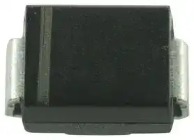
3.0SMCJ30A-13
TVS Diode, Unidirectional, 30 V, 48.4 V, DO-214AB (SMC), 2 Pins
⚠️ Reference pricing provided. In case of supply shortages, we will connect you with our trusted procurement partners to ensure your project's continuity.
- Manufacturer: DIODES INC.
- Product type: TVS Diodes
- SVHC: Lead (25-Jun-2025)
- No. of Pins: 2Pins
- TVS Polarity: Unidirectional
- Product Range: -
- Qualification: -
- Diode Mounting: Surface Mount
- Diode Case Style: DO-214AB (SMC)
- Clamping Voltage Max: 48.4V
- Reverse Standoff Voltage: 30V
- Maximum Breakdown Voltage: 36.8V
- Minimum Breakdown Voltage: 33.3V
- Operating Temperature Max: 150°C
- Peak Pulse Power Dissipation: 3kW
| Delivery and price | |
|---|---|
| Units per pack | 1000 |
| Price | 0.286 € |
| Current stock | 1000+ |
| Lead time | 30 days |
Datasheet

## **3.0SMCJ5.0(C)A – 3.0SMCJ170(C)A** ee — **3000W SURFACE MOUNT TRANSIENT VOLTAGE SUPPRESSOR**

## **Product Summary**

|**PPK**|**VRWM**|**PM(AV)**|
|---|---|---|
|3000W|5V to 170V|5W|


## **Features and Benefits**

- 3000W Peak Pulse Power Dissipation

- 5V to 170V Standoff Voltages

- Unidirectional and Bidirectional

- Glass Passivated Die Construction

- Excellent Clamping Capability

- **Lead-Free Finish; RoHS Compliant (Notes 1 & 2)**

- **Halogen and Antimony Free. “Green” Device (Note 3)**

- **For automotive applications requiring specific change control (i.e.: parts qualified to AEC-Q100/101/200, PPAP capable, and manufactured in IATF 16949 certified facilities), please refer to the related automotive grade (Q-suffix) part. A listing can be found at**

   -

   - **https://www.diodes.com/products/automotive/automotive products/.**

- **This part is qualified to JEDEC standards (as references in AEC-Q) for High Reliability. https://www.diodes.com/quality/product-definitions/**

## **Mechanical Data**

- Package: SMC

- Package Material: Molded Plastic. UL Flammability Classification Rating 94V-0

- Moisture Sensitivity: Level 1 per J-STD-020

- Terminals: Finish - Matte Tin Plated Leads. Solderable per MIL-STD-202, Method 208

- Unidirectional Devices Have A Cathode Band. Bidirectional Devices Have No Polarity Indicator

- Weight: 0.21 grams (Approximate)

SMC

Top View

Bottom View

## **Ordering Information** (Note 4)

|**Ordering Informationg Information Information**(Note 4)|**Ordering Informationg Information Information**(Note 4)|**Ordering Informationg Information Information**(Note 4)|**Ordering Informationg Information Information**(Note 4)|**Ordering Informationg Information Information**(Note 4)|
|---|---|---|---|---|
||||||
|**Part Number**|**Qualification**|**Package**|**Packing**||
||||**Qty. **|**Carrier**|
|3.0SMCJX.X(C)A-13*|Commercial|SMC|3000pcs|Tape & Reel|
|3.0SMCJXX(C)A-13*|Commercial|SMC|3000pcs|Tape & Reel|
|3.0SMCJXXX(C)A-13*|Commercial|SMC|3000pcs|Tape & Reel|


- *X = Device Voltage, e.g., 3.0SMCJ14CA-13.

- Notes: 1. EU Directive 2002/95/EC (RoHS), 2011/65/EU (RoHS 2) & 2015/863/EU (RoHS 3) compliant. All applicable RoHS exemptions applied.

   2. See https://www.diodes.com/quality/lead-free/ for more information about Diodes Incorporated’s definitions of Halogen- and Antimony-free, "Green" and Lead-free.

   3. Halogen- and Antimony-free "Green” products are defined as those which contain <900ppm bromine, <900ppm chlorine (<1500ppm total Br + Cl) and <1000ppm antimony compounds.

   4. For packaging details, go to our website at https://www.diodes.com/design/support/packaging/diodes-packaging/.

1 of 6

3.0SMCJ5.0(C)A – 3.0SMCJ170(C)A Document number: DS30818 Rev. 16 - 2

October 2021 © Diodes Incorporated

**www.diodes.com**

**3.0SMCJ5.0(C)A – 3.0SMCJ170(C)A**

## **Marking Information**

**==> picture [171 x 64] intentionally omitted <==**

**----- Start of picture text -----**<br>
Cathode Band for Uni- Bi-Directional Device<br>Directional Device<br>  YWW YWW  YWW<br>XXX  xxx XXX<br>**----- End of picture text -----**<br>


XXX = Product Type Marking Code (See Electrical Characteristics Table) = Manufacturers’ Marking YWW = Date Code Marking Y = Last Digit of Year (ex: 1 for 2021) WW = Week Code (01 to 53)

## **Maximum Ratings** (@ TA = +25°C, unless otherwise specified.)

|**Characteristic**|**Symbol**|**Value**|**Unit**|
|---|---|---|---|
|Peak Pulse Power Dissipation (Note 5)|PPK|3000|W|
|Peak Forward Surge Current, 8.3ms<br>Single Half Sine Wave Superimposed on Rated Load(Notes 6 & 7 & 8)|IFSM|300|A|


Notes: 5. Non-repetitive current pulse per Figure 4 and derated above TA = +25°C per Figure 1. 6. Mounted on 8.00mm[2] (0.013mm thick) land areas.

7. Measured with 8.3ms single half sine-wave. Duty cycle = 4 pulses per minute maximum.

8. Unidirectional units only.

## **Thermal Characteristics**

|**Thermal Characteristics**|**Thermal Characteristics**|**Thermal Characteristics**|**Thermal Characteristics**|
|---|---|---|---|
|||||
|**Characteristic**|**Symbol**|**Value**|**Unit**|
|OperatingTemperature Range|TJ|-55 to +150|°C|
|Storage Temperature Range|TSTG|-55 to +150|°C|


2 of 6 **www.diodes.com**

3.0SMCJ5.0(C)A – 3.0SMCJ170(C)A Document number: DS30818 Rev. 16 - 2

October 2021 © Diodes Incorporated

**3.0SMCJ5.0(C)A – 3.0SMCJ170(C)A**

**Electrical Characteristics** (@ TA = +25°C, unless otherwise specified.)

|**Electrical Characteristics**(@ TA = +25°C, unless otherwise specified.)A = +25°C, unless otherwise specified.)= +25°C, unless otherwise specified.)|**Electrical Characteristics**(@ TA = +25°C, unless otherwise specified.)A = +25°C, unless otherwise specified.)= +25°C, unless otherwise specified.)|**Electrical Characteristics**(@ TA = +25°C, unless otherwise specified.)A = +25°C, unless otherwise specified.)= +25°C, unless otherwise specified.)|**Electrical Characteristics**(@ TA = +25°C, unless otherwise specified.)A = +25°C, unless otherwise specified.)= +25°C, unless otherwise specified.)|**Electrical Characteristics**(@ TA = +25°C, unless otherwise specified.)A = +25°C, unless otherwise specified.)= +25°C, unless otherwise specified.)|**Electrical Characteristics**(@ TA = +25°C, unless otherwise specified.)A = +25°C, unless otherwise specified.)= +25°C, unless otherwise specified.)|**Electrical Characteristics**(@ TA = +25°C, unless otherwise specified.)A = +25°C, unless otherwise specified.)= +25°C, unless otherwise specified.)|**Electrical Characteristics**(@ TA = +25°C, unless otherwise specified.)A = +25°C, unless otherwise specified.)= +25°C, unless otherwise specified.)|**Electrical Characteristics**(@ TA = +25°C, unless otherwise specified.)A = +25°C, unless otherwise specified.)= +25°C, unless otherwise specified.)|**Electrical Characteristics**(@ TA = +25°C, unless otherwise specified.)A = +25°C, unless otherwise specified.)= +25°C, unless otherwise specified.)|
|---|---|---|---|---|---|---|---|---|---|
|||||||||||
|**Part Number**<br>~~—ptf~~|**Reverse**<br>**Standoff**<br>**Voltage**<br>~~ptf~~|**Breakdown**<br>**Voltage**<br>**VBR @ IT (Note 10)**<br>~~ptf~~||**Test**<br>**Current**<br>~~ptf~~|**Max.**<br>**Reverse**<br>**Leakage @**<br>**VRWM**<br>**(Note 11)**<br>~~tf~~|**Max. Clamping**<br>**Voltage @ IPP**<br>**(Note 9)**<br>~~tf~~|**Max.**<br>**Peak**<br>**Pulse**<br>**Current**<br>~~tf~~|**Marking Code**<br>~~tf~~||
||**VRWM (V)**<br>~~ptf~~|**Min(V)**<br>~~ptf~~|**Max(V)**<br>~~ptf~~|**IT (mA)**<br>~~ptf~~|**IR (µA)**<br>~~tf~~|**VC (V)**<br>~~tf~~|**Ipp (A)**<br>~~tf~~|**Un-**<br>~~tf~~|**Bi-**<br>~~tf~~|
|3.0SMCJ5.0(C)A<br>~~—ptf~~|5.0<br>~~ptf~~|6.40<br>~~ptf~~|7.07<br>~~ptf~~|10<br>~~ptf~~|1000<br>~~tf~~|9.2<br>~~tf~~|326.1<br>~~tf~~|HDE<br>~~tf~~|DHS<br>~~tf~~|
|3.0SMCJ6.0(C)A<br>~~—ptf~~|6.0<br>~~ptf~~|6.67<br>~~ptf~~|7.37<br>~~ptf~~|10<br>~~ptf~~|1000<br>~~tf~~|10.3<br>~~tf~~|291.3<br>~~tf~~|HDG<br>~~tf~~|DDG<br>~~tf~~|
|3.0SMCJ6.5(C)A<br>~~— ptf~~|6.5<br>~~ptf~~|7.22<br>~~ptf~~|7.98<br>~~ptf~~|10<br>~~ptf ~~|500<br> ~~tf~~|11.2<br>~~tf~~|267.9<br>~~tf~~|HDK<br>~~tf~~|DHV<br>~~tf~~|
|3.0SMCJ7.0(C)A|7.0|7.78|8.60|10|200|12.0|250.0|HDM|DHW|
|3.0SMCJ7.5(C)A|7.5|8.33|9.21|1.0|100|12.9|232.6|HDP|DDP|
|3.0SMCJ8.0(C)A|8.0|8.89|9.83|1.0|50|13.6|220.6|HDR|DDR|
|3.0SMCJ8.5(C)A|8.5|9.44|10.43|1.0|25|14.4|208.3|HDT|DDT|
|3.0SMCJ9.0(C)A|9.0|10.00|11.05|1.0|10|15.4|194.8|HDV|DDV|
|3.0SMCJ10(C)A|10.0|11.10|12.27|1.0|5.0|17.0|176.5|HDX|DDX|
|3.0SMCJ11(C)A|11.0|12.20|13.5|1.0|5.0|18.2|164.8|HDZ|DDZ|
|3.0SMCJ12(C)A|12.0|13.30|14.7|1.0|5.0|19.9|150.8|HEE|DEE|
|3.0SMCJ13(C)A|13.0|14.40|15.9|1.0|5.0|21.5|139.5|HEG|DED|
|3.0SMCJ14(C)A|14.0|15.60|17.2|1.0|5.0|23.2|129.3|HDE|DEK|
|3.0SMCJ15(C)A|15.0|16.70|18.5|1.0|5.0|24.2|124.0|HEM|DEM|
|3.0SMCJ16(C)A|16.0|17.80|19.7|1.0|5.0|26.0|115.4|HEP|DEP|
|3.0SMCJ17(C)A|17.0|18.90|20.9|1.0|5.0|27.6|108.7|HER|DER|
|3.0SMCJ18(C)A|18.0|20.00|22.1|1.0|5.0|29.2|102.7|HET|DET|
|3.0SMCJ20(C)A|20.0|22.20|24.5|1.0|5.0|32.4|92.6|HEV|DEV|
|3.0SMCJ22(C)A|22.0|24.40|27.0|1.0|5.0|35.5|84.5|HEX|DEX|
|3.0SMCJ24(C)A|24.0|26.70|29.5|1.0|5.0|38.9|77.1|HEZ|DEZ|
|3.0SMCJ26(C)A|26.0|28.90|31.9|1.0|5.0|42.1|71.3|HFE|DFE|
|3.0SMCJ28(C)A|28.0|31.10|34.4|1.0|5.0|45.4|66.1|HFG|DFD|
|3.0SMCJ30(C)A|30.0|33.30|36.8|1.0|5.0|48.4|62.0|HFK|DFK|
|3.0SMCJ33(C)A|33.0|36.70|40.6|1.0|5.0|53.3|56.3|HFM|DFM|
|3.0SMCJ36(C)A|36.0|40.00|44.2|1.0|5.0|58.1|51.6|HFP|DFP|
|3.0SMCJ40(C)A|40.0|44.40|49.1|1.0|5.0|64.5|46.5|HFR|DFR|
|3.0SMCJ43(C)A|43.0|47.80|52.8|1.0|5.0|69.4|43.2|HFT|DFT|
|3.0SMCJ45(C)A|45.0|50.00|55.3|1.0|5.0|72.7|41.3|HFV|DFV|
|3.0SMCJ48(C)A|48.0|53.30|58.9|1.0|5.0|77.4|38.8|HFX|DFX|
|3.0SMCJ51(C)A|51.0|56.70|62.7|1.0|5.0|82.4|36.4|HFZ|DFZ|
|3.0SMCJ54(C)A|54.0|60.00|66.3|1.0|5.0|87.1|34.4|HGE|DDE|
|3.0SMCJ58(C)A|58.0|64.40|71.2|1.0|5.0|93.6|32.1|HGG|DDD|
|3.0SMCJ60(C)A|60.0|66.70|73.7|1.0|5.0|96.8|31.0|HGK|DDK|
|3.0SMCJ64(C)A|64.0|71.10|78.6|1.0|5.0|103.0|29.1|HGM|DDM|
|3.0SMCJ70(C)A|70.0|77.80|86.0|1.0|5.0|113.0|26.5|HGP|DGP|
|3.0SMCJ75(C)A|75.0|83.30|92.1|1.0|5.0|121.0|24.8|HGR|DGR|
|3.0SMCJ78(C)A|78.0|86.70|95.8|1.0|5.0|126.0|23.8|HGT|DGT|
|3.0SMCJ85(C)A|85.0|94.40|104.3|1.0|5.0|137.0|21.9|HGV|DGV|
|3.0SMCJ90(C)A|90.0|100.00|110.5|1.0|5.0|146.0|20.5|HGX|DGX|
|3.0SMCJ100(C)A|100.0|111.00|122.7|1.0|5.0|162.0|18.5|HGZ|DGZ|
|3.0SMCJ110(C)A|110.0|122.00|134.8|1.0|5.0|177.0|16.9|HHE|DHE|
|3.0SMCJ120(C)A|120.0|133.00|147.0|1.0|5.0|193.0|15.5|HHG|DHG|
|3.0SMCJ130(C)A|130.0|144.00|159.2|1.0|5.0|209.0|14.4|HHK|DHK|
|3.0SMCJ150(C)A|150.0|167.00|184.6|1.0|5.0|243.0|12.3|HHM|DGM|
|3.0SMCJ160(C)A|160.0|178.00|196.7|1.0|5.0|259.0|11.6|HHP|DHP|
|3.0SMCJ170(C)A|170.0|189.00|208.9|1.0|5.0|275.0|10.9|HHR|DHR|


- Notes: 9. Per 10 × 1000μs waveform. See Figure 2.

   10. VBR measured with IT current pulse = 10ms to 15ms.

   11. The IR limit is double for Bi-Directional device for VB ≦ 10V.

3 of 6 **www.diodes.com**

3.0SMCJ5.0(C)A – 3.0SMCJ170(C)A Document number: DS30818 Rev. 16 - 2

October 2021 © Diodes Incorporated

**3.0SMCJ5.0(C)A – 3.0SMCJ170(C)A**

**==> picture [468 x 453] intentionally omitted <==**

**----- Start of picture text -----**<br>
125100 he i e Sf<br>10X1000 Waveform as Defined by REA<br>75<br>50 50<br>25<br>| ae<br>0 as defined by R EA.<br>0 25 50 75 100 125 150 175 0 0 Ptnase 1 2 7 3<br>TA, AMBIENT TEMPERATURE (°C) Fig. 2 Pulse Waveformt, TIME (ms)<br>Fig. 1 Pulse Derating Curve Figure 1 Pulse Derating Curve<br>100 Seti)aa 300 8.3ms Single Half-Sine-Wave<br>SSeS SA<br>|Seeti nohl eeeMt 250 Na | |<br>Non Repetitive  Non Repetitive<br>SO Pulse Waveform  Pulse Waveform | x<br>Shown in Fig.2  Shown in Fig. 4<br>10 || a_— iH 200 IN \<br>a a aaS | 150 s NU<br>1.0 SaOaa anaa a |EL Sa 100 INST™ LLU<br>Eee a a aena || |TH<br>50<br>0.1 0<br>0.1 1.0 10 100 1,000 10,000 1 2 5 10 20 50 100<br>Fig. 3 Pulse Rating Curvetp PULSE WIDTH  ( 祍μs ) Fig. 4 Maximum Non-Repetitive Surge CurrentNUMBER OF CYCLES AT 60Hz<br>PEAK FORWARD SURGE CURRENT (A)<br>IFSM,<br>pp<br>PP<br>)<br>, PEAK PULSE CURRENT (%I<br>I<br>, PEAK PULSE POWER (kW)<br>D<br>P<br> PEAK PULSE DERATING IN %  OF PEAK POWER OR CURRENT<br>**----- End of picture text -----**<br>


4 of 6 **www.diodes.com**

3.0SMCJ5.0(C)A – 3.0SMCJ170(C)A Document number: DS30818 Rev. 16 - 2

October 2021

© Diodes Incorporated

**3.0SMCJ5.0(C)A – 3.0SMCJ170(C)A**

## **Package Outline Dimensions**

Please see http://www.diodes.com/package-outlines.html for the latest version.

**==> picture [21 x 7] intentionally omitted <==**

**----- Start of picture text -----**<br>
SMC<br>**----- End of picture text -----**<br>


**==> picture [310 x 157] intentionally omitted <==**

**----- Start of picture text -----**<br>
|||||||
|---|---|---|---|---|---|
|B|
|SMC|
|Dim|Min|Max|
|ap|—|A|5.59|6.22|
|A|C|B|6.60|7.11|
|C|2.75|3.18|
|D|0.15|0.31|
|:|[;]|
|E|7.75|8.13|
|G|0.10|0.20|
|T|rT|D|H J|02..7006|1.2.5502|
|J|
|All Dimensions in mm|
|—e|
|H|G|
|E|
|—|

**----- End of picture text -----**<br>


## **Suggested Pad Layout**

Please see http://www.diodes.com/package-outlines.html for the latest version.

**SMC**

**==> picture [167 x 108] intentionally omitted <==**

**----- Start of picture text -----**<br>
X1<br>X<br>Ee<br>Y<br>G<br>LS C<br>**----- End of picture text -----**<br>


**==> picture [95 x 65] intentionally omitted <==**

**----- Start of picture text -----**<br>
|||
|---|---|
|Value|
|Dimensions|
|(in mm)|
|C|6.90|
|G|4.40|
|X|2.50|
|X1|9.40|
|Y|3.30|

**----- End of picture text -----**<br>


5 of 6 **www.diodes.com**

3.0SMCJ5.0(C)A – 3.0SMCJ170(C)A Document number: DS30818 Rev. 16 - 2

October 2021 © Diodes Incorporated

**3.0SMCJ5.0(C)A – 3.0SMCJ170(C)A**

## **IMPORTANT NOTICE**

1. DIODES INCORPORATED AND ITS SUBSIDIARIES (“DIODES”) MAKE NO WARRANTY OF ANY KIND, EXPRESS OR IMPLIED, WITH REGARDS TO ANY INFORMATION CONTAINED IN THIS DOCUMENT, INCLUDING, BUT NOT LIMITED TO, THE IMPLIED WARRANTIES OF MERCHANTABILITY, FITNESS FOR A PARTICULAR PURPOSE OR NON-INFRINGEMENT OF THIRD PARTY INTELLECTUAL PROPERTY RIGHTS (AND THEIR EQUIVALENTS UNDER THE LAWS OF ANY JURISDICTION).

2. The Information contained herein is for informational purpose only and is provided only to illustrate the operation of Diodes products described herein and application examples. Diodes does not assume any liability arising out of the application or use of this document or any product described herein. This document is intended for skilled and technically trained engineering customers and users who design with Diodes products. Diodes products may be used to facilitate safety-related applications; however, in all instances customers and users are responsible for (a) selecting the appropriate Diodes products for their applications, (b) evaluating the suitability of the Diodes products for their intended applications, (c) ensuring their applications, which incorporate Diodes products, comply the applicable legal and regulatory requirements as well as safety and functional-safety related standards, and (d) ensuring they design with appropriate safeguards (including testing, validation, quality control techniques, redundancy, malfunction prevention, and appropriate treatment for aging degradation) to minimize the risks associated with their applications.

3. Diodes assumes no liability for any application-related information, support, assistance or feedback that may be provided by Diodes from time to time. Any customer or user of this document or products described herein will assume all risks and liabilities associated with such use, and will hold Diodes and all companies whose products are represented herein or on Diodes’ websites, harmless against all damages and liabilities.

4. Products described herein may be covered by one or more United States, international or foreign patents and pending patent applications. Product names and markings noted herein may also be covered by one or more United States, international or foreign trademarks and trademark applications. Diodes does not convey any license under any of its intellectual property rights or the rights of any third parties (including third parties whose products and services may be described in this document or on Diodes’ website) under this document.

5. Diodes products are provided subject to Diodes’ Standard Terms and Conditions of Sale (https://www.diodes.com/about/company/terms-and-conditions/terms-and-conditions-of-sales/) or other applicable terms. This document does not alter or expand the applicable warranties provided by Diodes. Diodes does not warrant or accept any liability whatsoever in respect of any products purchased through unauthorized sales channel.

6. Diodes products and technology may not be used for or incorporated into any products or systems whose manufacture, use or sale is prohibited under any applicable laws and regulations. Should customers or users use Diodes products in contravention of any applicable laws or regulations, or for any unintended or unauthorized application, customers and users will (a) be solely responsible for any damages, losses or penalties arising in connection therewith or as a result thereof, and (b) indemnify and hold Diodes and its representatives and agents harmless against any and all claims, damages, expenses, and attorney fees arising out of, directly or indirectly, any claim relating to any noncompliance with the applicable laws and regulations, as well as any unintended or unauthorized application.

7. While efforts have been made to ensure the information contained in this document is accurate, complete and current, it may contain technical inaccuracies, omissions and typographical errors. Diodes does not warrant that information contained in this document is error-free and Diodes is under no obligation to update or otherwise correct this information. Notwithstanding the foregoing, Diodes reserves the right to make modifications, enhancements, improvements, corrections or other changes without further notice to this document and any product described herein. This document is written in English but may be translated into multiple languages for reference. Only the English version of this document is the final and determinative format released by Diodes.

8. Any unauthorized copying, modification, distribution, transmission, display or other use of this document (or any portion hereof) is prohibited. Diodes assumes no responsibility for any losses incurred by the customers or users or any third parties arising from any such unauthorized use.

Copyright © 2021 Diodes Incorporated

**www.diodes.com**

6 of 6 **www.diodes.com**

3.0SMCJ5.0(C)A – 3.0SMCJ170(C)A Document number: DS30818 Rev. 16 - 2

October 2021 © Diodes Incorporated
Updated at April 26, 2026
About Novapart
Novapart is a B2B electronic component broker specialising in stock shortages and cost reduction. We source hard-to-find parts and identify compliant alternatives across a catalogue of 410,000+ components from 500+ manufacturers.
Learn more →Stock Shortage Specialist
When a component is unavailable, discontinued or has an unacceptable lead time, we tap into our network of vetted European and Asian distributors to source what you need — without compromising on quality or traceability.
Request a quote →Compliant Alternatives
We identify pin-to-pin, electrically equivalent substitutes that meet the same certifications (RoHS, AEC-Q100, REACH) as your original specification — validated against datasheets, not just part numbers. Often at a lower cost.
BOM Analysis service →