


2SK3065T100
Power MOSFET, N Channel, 60 V, 2 A, 0.32 ohm, SOT-89, Surface Mount
- Manufacturer: ROHM
- Product type: Single MOSFETs
- Transistor Polarity:N Channel; Continuous Drain Current Id:2A; Drain Source Voltage Vds:60V; On Resistance Rds(on):0.25ohm; Rds(on) T; Available until stocks are exhausted Alternative available
- MSL: MSL 1 - Unlimited
- SVHC: Lead (23-Jan-2024)
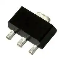
- No. of Pins: 3Pins
- Channel Type: N Channel
- Product Range: -
- Qualification: -
- Power Dissipation: 500mW
- Transistor Mounting: Surface Mount
- Rds(on) Test Voltage: 4V
- Transistor Case Style: SOT-89
- Drain Source Voltage Vds: 60V
- Operating Temperature Max: 150°C
- Continuous Drain Current Id: 2A
- Drain Source On State Resistance: 0.32ohm
- Gate Source Threshold Voltage Max: 800mV
| Delivery and price | |
|---|---|
| Units per pack | 200 |
| Price | 0.376 € |
| Current stock | 200+ |
| Lead time | 30 days |
2SK3065 Transistors ## Small switching (60V, 2A) ## **2SK3065** ## ! **Features** ## ! **External dimensions** (Units : mm) - 1) Low on resistance. 2) High-speed switching. 3) Optimum for a pocket resource etc. because of undervoltage actuation (2.5V actuation). - 4) Driving circuit is easy. - 5) Easy to use parallel. - 6) It is strong to an electrostatic discharge. ## ! **Structure** **==> picture [195 x 85] intentionally omitted <==** **----- Start of picture text -----**<br> 4.5 +− 0.20.1<br>1.6 ± 0.1 1.5 ± 0.1<br>(1) (2) (3) 0.4 +− 0.10.05<br>0.4 ± 0.1 0.5 ± 0.1 0.4 ± 0.1<br>1.5 ± 0.1 1.5 ± 0.1<br>3.0 ± 0.2<br>(1) Gate<br>ROHM : MPT3 Abbreviated symbol : KE (2) Drain<br>E I A J : SC-62 (3) Source<br>0.10.5 ±<br>0.5 + 4.00.3 − 0.2 + 2.50.1 −<br>0.31.0 ±<br>**----- End of picture text -----**<br> Silicon N-channel MOS FET transistor ! **Absolute maximum ratings** (Ta = 25°C) Parameter Symbol Limits Unit Drain-source voltage VDSS 60 V Gate-source voltage VGSS ± 20 V Continuous ID 2 A Drain current Pulsed IDP[∗][1] 8 A Reverse drain Continuous IDR 2 A current Pulsed IDRP[∗][1] 8 A Total power dissipation(Tc=25 ° C) PD 0.52[∗][2] W Channel temperature Tch 150 ° C TE Storage temperature Tstg − 55 ∼+ 150 ° C ∗ 1 Pw ≤ 10 µ s, Duty cycle ≤ 1% ∗ 2 When mounted on a 40 × 40 × 0.7 mm alumina board. ## ! **Internal equivalent circuit** **==> picture [90 x 93] intentionally omitted <==** **----- Start of picture text -----**<br> Drain<br>Gate<br> ∗ Gate<br> Protection<br> Diode Source<br>**----- End of picture text -----**<br> ∗ A protection diode has been built in between the gate and the source to protect against static electricity when the product is in use. Use the protection circuit when rated voltages are exceeded. ## ! **Electrical characteristics** (Ta = 25°C) |Parameter|Symbol|Min.|Typ.|Max.|Unit|Test Conditions| |---|---|---|---|---|---|---| |Gate-source leakage|IGSS|−|−|±10|µA|VGS=±20V, VDS=0V| |Drain-source breakdown voltage|V(BR)DSS|60|−|−|V|ID=1mA, VGS=0V| |Zero gate voltage drain current|IDSS|−|−|10|µA|VDS=60V, VGS=0V| |Gate threshold voltage|VGS(th)|0.8|−|1.5|V|VDS=10V, ID=1mA| |Static drain-source on-state<br>resistance|RDS(on)|−|0.25|0.32|Ω|ID=1A, VGS=4V| ||RDS(on)|−|0.35|0.45|Ω|ID=1A, VGS=2.5V| |Forward transfer admittance|Yfs∗|1.5|−|−|S|ID=1A, VDS=10V| |Input capacitance|Ciss|−|160|−|pF|VGS=0V<br>f=1MHz<br>VDS=10V| |Output capacitance|Coss|−|85|−|pF|| |Reverse transfer capacitance|Crss|−|25|−|pF|| |Turn-on delay time|td(on)|−|20|−|ns|VGS=4V<br>ID=1A, VDD30V<br>RL=30Ω<br>RG=10Ω| |Rise time|tr|−|50|−|ns|| |Turn-off delaytime|td(off)|−|120|−|ns|| |Fall time|tf|−|70|−|ns|| ∗[ Pw ][≤ ][300][µ][s, Duty cycle ][≤ ][1%] 2SK3065 ## Transistors ! **Packaging specifications** Package Taping Code T100 Type Basic ordering unit (pieces) 1000 2SK3065 = ~~F~~ ## ! **Electrical characteristic curves** **==> picture [435 x 371] intentionally omitted <==** **----- Start of picture text -----**<br> 3 10 Operating in this 100 µ s 2 4V Ta=25 ° C<br>When mounted on a 40 x 40 x 0.7 mmaluminum-ceramic board. area is limited byRDS(on) 1ms 3V3.5V Pulsed<br>1 Pw = 10ms 2.5V<br>2<br>2V<br>0.1 a DC OPERATION Nl 1 yy | bt TTT<br>1<br>0.01<br>Ta = 25 ° C<br>Single Pulsed VGS=1.5V<br>0 PPh 0.001 Fun THe) =| R 0 EE<br>0 25 50 75 100 125 150 175 0.1 1 10 100 0 5 10<br>AMBIENT TEMPERATURE : Ta( ° C) DRAIN-SOURCE VOLTAGE : VDS(V) DRAIN-SOURCE VOLTAGE : VDS(V)<br>Fig.1 Total Power Dissipation vs. Fig.2 Maximum Safe Operating Area Fig.3 Typical Output Characteristics<br>Case Temperature<br>10 VDS=10V 4 VDS=10V 10 VGS=4V<br>Pulsed Pulsed<br>YT | |[|PD, [| 3 a<br>ae a Ta= − 25 ° C a a Ta=125 ° C |<br>1 2575 °° CC 2 1 75 25 °° CC<br>125 ° C 10mA − 25 ° C<br>ee | ee 1 a<br>ID=1mA<br>0.10 i 1 2 3 4 5 0 − 50 − 25 0 25 50 75 100 125 150 0.10.01 Tt 0.1 Th 1 nell 10<br>GATE THRESHOLD VOLTAGE : VGS(th)(V) CHANNEL TEMPERATURE : Tch( ° C) DRAIN CURRENT : ID(A)<br>Fig.4 Typical Transfer Characteristics Fig.5 Gate Threshold Voltage vs.<br>Channel Temperature Fig.6 Static Drain-Source On-<br>State Resistance vs.<br>Drain Current( Ι )<br>(W)D<br>DRAIN CURRENT : I(A)D DRAIN CURRENT : I(A)D<br>TOTAL POWER DISSIPATION : P<br>V)<br>(th)( ) Ω<br>GS (on)(<br>DRAIN CURRENT : I(A)D DS<br>GATE THRESHOLD VOLTAGE : V STATIC DRAIN-SOURCE ON-STATE RESISTANCE : R<br>**----- End of picture text -----**<br> 2SK3065 Transistors **==> picture [434 x 559] intentionally omitted <==** **----- Start of picture text -----**<br> 10 VGS=2.5V 1 Ta=25 ° C 1 VGS=4V<br>SSKe too Pulsed || Pulsed | Pulsed |<br>CreYt 0.75 | | na<br>Ta=125 ° C 2A<br>1 STtMee ayl − 75 2525 °°° CCC Illoe 0.5 qe||a ID=1A | 0.5 PEEL E 2A pyLE<br>EeeeTSt \( Lrra<br>0.25<br>ID=1A<br>0.10.01 Pfitecttetm 0.1 1 10 «=| LL 00 5 EE] 10 15 20 | 0 − 50 CLEL − 25 0 25 50 75 L 100 L 125 150<br>DRAIN CURRENT : ID(A) GATE-SOURCE VOLTAGE : VGS(V) CHANNEL TEMPERATURE : Tch( ° C)<br>Fig.7 Static Drain-Source On- Fig.8 Static Drain-Source On- Fig.9 Static Drain-Source On-<br>State Resistance vs. State Resistance vs. State Resistance vs.<br>Drain Current( ΙΙ ) Gate-Source Voltage Channel Temperature<br>10 VDS=10V 10 VGS=4V 10 Ta=25 ° C<br>EE Pulsed oo ———— Pulsed ———— Pulsed<br>p Ta= − 25 ° C h po }—_}—}—_ | |_| 4<br>mae 25 ° C CN ZAI 1 } | ft f yey ft yf 1 ee 4V eee<br>ae 125 ° C Se8)//(2e8 e r f || |<br>1 PoIL AAA A 75 ° C ll SSSees Ta=125 75 25 = °°° CCC — === oe V —— GS=0V ——<br>0.1 − 25 ° C 0.1<br>YY, F< Fe _— SF<br>Zo) dR EEREEEE<br>0.10.01 ABA 0.1 1 10 0.010 TP 0.4 0.8 1.2 1.6 0.010 Ss 0.4 0.8 1.2 1.6<br>DRAIN CURRENT : ID(A) SOURCE-DRAIN VOLTAGE : VSD(V) SOURCE-DRAIN VOLTAGE : VSD(V)<br>Fig.10 Forward Trasfer Admitance vs. Fig.11 Reverse Drain Current vs. Fig.12 Reverse Drain Current vs.<br>Drain Current Source-Drain Voltage( Ι ) Source-Drain Voltage( ΙΙ )<br>1000 1000 1000<br>VGS=0V VDD 30V di/dt=50A/ µ s<br>===... f=1MHZ Fee VGS=4V -— eet VGS=0V<br>—— Ta=25 ° C FF J RG=10 Ω a Ta=25 ° C<br>_— a Ciss t d Pr Ta=25 ° C a Pulsed<br>paw Ln Pulsed PT<br>100<br>PP e ar l P T td(off) a i<br>S SS Coss 100 IH U II 100 ll<br>PS >) SSH | NR A pf tt<br>ee e a tf Err EH<br>10 CSSS Sess: o Crss —— ===: «= pe E t a r pT=eoT TTT TTT TTT<br>F t Ltr el Pt TT TT<br>10 Sereda 10 ee 100 100.1 | td(on)1 10 100.1 1 10<br>DRAIN-SOURCE VOLTAGE : VSD(V) DRAIN CURRENT : ID(A) REVERSE DRAIN CURRENT : IDR(A)<br>Fig.13 Typical Capacitance vs. Fig.14 Switching Characteristics Fig.15 Reverse Recovery Time vs.<br>Drain-Source Voltage (a measurement circuit diagram Fig.17 , it refers 18 times) Reverse Drain Current<br>) Ω ) Ω ) Ω<br>(on)( (on)( (on)(<br>DS DS DS<br>STATIC DRAIN-SOURCE ON-STATE RESISTANCE : R STATIC DRAIN-SOURCE ON-STATE RESISTANCE : R STATIC DRAIN-SOURCE ON-STATE RESISTANCE : R<br>(A) (A)<br>DR DR<br>REVERSE DRAIN CURRENT : I REVERSE DRAIN CURRENT : I<br>FORWARD TRANSFER ADMITTANCE : | Yfs |(S)<br>CAPACITANCE : C(pF) SWITCHING TIME : t(ns)<br>REVERSE RECOVERY TIME : trr(ns)<br>**----- End of picture text -----**<br> 2SK3065 Transistors **==> picture [248 x 131] intentionally omitted <==** **----- Start of picture text -----**<br> 10<br>PTa0 [TTT] ee<br>D=1<br>1 e 0.5 tTy<br>EEEEE<br>0.1 Pe e 0.20.1 0ee trie When mounted on a 40 x 40 x 0.7 mm tt ttt|<br>0.05<br>aluminum-ceramic board.<br>ESeS 0.02 tt Ta=25 ° C ttl<br>0.01 pesee 0.01 edFTALL GREECTEee TTL ee θθ th (ch-c) th (ch-c) (t) =62.5= r (t) ° C/W • θ th (ch-c)<br>pr Single pulse eee<br>Po pe PW qy T u D= b PWT<br>0.001 LT TTT TCT ETT TTT<br>100 µ 1m 10m 100m 1 10 100<br> PULSE WIDTH : PW(s)<br>NORMALIZED TRANSIENT THERMAL RESISTANCE : r(t)<br>**----- End of picture text -----**<br> Fig.16 Normarized Transient Thermal Resistance vs. Pulse Width ## ! **Switching characteristics measurement circuit** **==> picture [322 x 104] intentionally omitted <==** **----- Start of picture text -----**<br> Pulse width<br>90%<br>VGS ID VDS VGS 10%50% 50%<br>D.U.T. RL<br>RG VDS 10% 10%<br>VDD<br>90%<br>90%<br>td(on) tr tf<br>td(off)<br>ton toff<br>**----- End of picture text -----**<br> Fig.17 Switching Time Test Circuit Fig.18 Switching Time Waveforms
Updated at June 5, 2026
Founded with a steadfast commitment to a "Quality First" corporate policy, ROHM is a globally recognized leader in the design and manufacture of semiconductors and electronic components. Originally named for its foundational product, resistors, combined with the unit of resistance, the "R" in ROHM has evolved to represent the brand's enduring dedication to reliability. Today, the company is renowned for driving technological advancement and supplying high-performance, dependable solutions to engineers worldwide. The company's engineering excellence is most prominently showcased in its expansive portfolio of discrete semiconductors. ROHM provides an industry-leading selection of bipolar transistors, alongside a massive array of Zener single diodes, Schottky diodes, and small signal diodes. Engineered for rigorous efficiency and compact footprint requirements, these foundational components are critical for modern power management, precise signal processing, and high-speed switching applications. In addition to its core discrete offerings, ROHM delivers advanced power control and circuit protection solutions. This includes a highly trusted lineup of single and dual MOSFETs, single IGBTs, and transient voltage suppressors (TVS diodes) designed to safeguard sensitive circuitry. Complemented by intelligent power modules, precision sensors, and specialized ICs, ROHM equips designers with the premium components necessary to build the next generation of robust electronic infrastructure.
About Novapart
Novapart is a B2B electronic component broker specialising in stock shortages and cost reduction. We source hard-to-find parts and identify compliant alternatives across a catalogue of 410,000+ components from 500+ manufacturers.
Learn more →Stock Shortage Specialist
When a component is unavailable, discontinued or has an unacceptable lead time, we tap into our network of vetted European and Asian distributors to source what you need — without compromising on quality or traceability.
Request a quote →Compliant Alternatives
We identify pin-to-pin, electrically equivalent substitutes that meet the same certifications (RoHS, AEC-Q100, REACH) as your original specification — validated against datasheets, not just part numbers. Often at a lower cost.
BOM Analysis service →