
Image not available
Illustrative purposes only

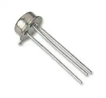
2N6845
Power MOSFET, P Channel, 100 V, 4 A, 0.6 ohm, TO-39, Through Hole
⚠️ Reference pricing provided. In case of supply shortages, we will connect you with our trusted procurement partners to ensure your project's continuity.
- Manufacturer: TT ELECTRONICS / SEMELAB
- Product type: Single MOSFETs
- No. of Pins: 3Pins
- Channel Type: P Channel
- Power Dissipation: 20W
- Transistor Mounting: Through Hole
- Transistor Polarity: P Channel
- Power Dissipation Pd: 20W
- Rds(on) Test Voltage: 10V
- On Resistance Rds(on): 0.6ohm
- Transistor Case Style: TO-39
- Drain Source Voltage Vds: 100V
- Operating Temperature Max: 150°C
- Continuous Drain Current Id: 4A
- Drain Source On State Resistance: 0.6ohm
- Gate Source Threshold Voltage Max: 4V
| Delivery and price | |
|---|---|
| Units per pack | 100 |
| Price | 24.85 € |
| Current stock | 10+ |
| Lead time | 30 days |
Datasheet

**2N6845 IRFF9120**

**==> picture [69 x 38] intentionally omitted <==**

## **MECHANICAL DATA**

Dimensions in mm (inches)

**==> picture [277 x 296] intentionally omitted <==**

**----- Start of picture text -----**<br>
8.64 (0.34)<br>9.40 (0.37)<br>8.01 (0.315)<br>9.01 (0.355)<br>4.06 (0.16)<br>4.57 (0.18)<br>0.89<br>12.70 (0.035) [max.]<br>(0.500)<br>min. 0.41 (0.016)<br>0.53 (0.021)<br>dia.<br>5.08 (0.200)<br>typ.<br>2.54<br>2 (0.100)<br>1 3<br>0.74 (0.029)<br>1.14 (0.045)<br>0.71 (0.028)<br>0.53 (0.021)<br>45°<br>**----- End of picture text -----**<br>


## **P–CHANNEL ENHANCEMENT MODE HIGH VOLTAGE POWER MOSFETS**

**V -100V DSS I -4.0A D(cont) R 0.60** Ω **DS(on)**

## **FEATURES**

- **HERMETICALLY SEALED TO–39 METAL PACKAGE**

- **SIMPLE DRIVE REQUIREMENTS**

- **LIGHTWEIGHT**

- **SCREENING OPTIONS AVAILABLE**

## **TO–39 (TO-205AF) METAL PACKAGE**

PIN1 – Source PIN 2 – Gate PIN 3 – Drain

## **ABSOLUTE MAXIMUM RATINGS** (Tcase = 25°C unless otherwise stated)

|VGS<br>Gate – Source Voltage<br>ID<br>Continuous Drain Current<br>(VGS= 0 , Tcase= 25°C)<br>ID<br>Continuous Drain Current<br>(VGS= 0 , Tcase= 100°C)<br>IDM<br>Pulsed Drain Current1<br>PD<br>Power Dissipation @ Tcase= 25°C<br>Linear Derating Factor<br>TJ, Tstg<br>Operating and Storage Temperature Range<br>TL<br>Package Mounting Surface Temperature (for 5 sec)<br>RθJC<br>Thermal Resistance Junction to Case|±20V<br>-4.0A<br>-2.6A<br>-16A<br>20 W<br>0.16 W/°C<br>–55 to 150°C<br>300°C<br>6.25°C/W||
|---|---|---|


## **Notes**

## 1)  Repetitive Rating – Pulse width limited by maximum junction temperature.

**Semelab Plc reserves the right to change test conditions, parameter limits and package dimensions without notice. Information furnished by Semelab is believed to be both accurate and reliable at the time of going to press. However Semelab assumes no responsibility for any errors or omissions discovered in its use. Semelab encourages customers to verify that datasheets are current before placing orders.**

**Semelab plc.** Telephone +44(0)1455 556565. Fax +44(0)1455 552612. E-mail: sales@semelab.co.uk Website: http://www.semelab.co.uk

Document Number 5748 Issue 2

**2N6845 IRFF9120**

**==> picture [69 x 38] intentionally omitted <==**

## **ELECTRICAL CHARACTERISTICS** (Tamb = 25°C unless otherwise stated)

**==> picture [539 x 512] intentionally omitted <==**

**----- Start of picture text -----**<br>
Parameter Test Conditions Min. Typ. Max. Unit<br>STATIC ELECTRICAL RATINGS<br>BVDSS Drain – Source Breakdown Voltage VGS = 0 ID = - 1mA - 100 V<br>∆BVDSS Temperature Coefficient of  Reference to 25°C<br>- 0.10 V/°C<br>∆TJ Breakdown Voltage ID = - 1mA<br>Static Drain – Source On–State VGS = - 10V ID = - 2.6A 0.60<br>R Ω<br>DS(on)<br>Resistance  [1] VGS = - 10V ID = - 4.0A 0.69<br>VGS(th) Gate Threshold Voltage VDS = VGS ID = -250µA - 2 - 4 V<br>gfs Forward Transconductance  [1] VDS > -15V ID = -2.6A 1.25 S<br>VDS = - 80V VGS = 0 -25<br>IDSS Drain-to-Source Leakage Current µA<br>TJ = 125°C -250<br>IGSS Forward Gate – Source Leakage VGS = 20V 100<br>nA<br>IGSS Reverse Gate – Source Leakage VGS = –20V -100<br>DYNAMIC CHARACTERISTICS<br>Ciss Input Capacitance VGS = 0 380<br>Coss Output Capacitance VDS = - 25V 170 pF<br>Crss Reverse Transfer Capacitance f = 1MHz 45<br>Qg Total Gate Charge VGS = -10V ID = -4.0A 4.3 16.3<br>Qgs Gate –  Source Charge VDS = -50V 1.3 4.7 nC<br>Qgd Gate –  Drain (“Miller”) Charge 1.0 9.0<br>td(on) Turn–On Delay Time VDD = -50V 60<br>tr Rise Time ID = - 4.0A 100<br>ns<br>td(off) Turn–Off Delay Time RG = 7.5Ω 50<br>tf Fall Time 70<br>SOURCE – DRAIN DIODE CHARACTERISTICS<br>IS Continuous Source Current Mosfet symbol showing the  D - 4.0<br>G A<br>ISM Pulse Source Current  integral reverse p-n junction diode S - 16<br>IS = - 4.0A TJ = 25°C<br>VSD Diode Forward Voltage [1] - 4.8 V<br>VGS = 0V<br>trr Reverse Recovery Time [1] IF = -4.0A TJ = 25°C 200 ns<br>Qrr Reverse Recovery Charge [1] di / dt ≤ -100A/µs VDD ≤ -50V 3.1 µC<br>ton Forward Turn–On Time Negligible<br>**----- End of picture text -----**<br>


## **Notes**

1)  Pulse Test: Pulse Width ≤ 300ms, δ ≤ 2%

**Semelab Plc reserves the right to change test conditions, parameter limits and package dimensions without notice. Information furnished by Semelab is believed to be both accurate and reliable at the time of going to press. However Semelab assumes no responsibility for any errors or omissions discovered in its use. Semelab encourages customers to verify that datasheets are current before placing orders.**

**Semelab plc.**

Telephone +44(0)1455 556565. Fax +44(0)1455 552612. E-mail: sales@semelab.co.uk Website: http://www.semelab.co.uk

Document Number 5748 Issue 2
Updated at February 9, 2023
About Novapart
Novapart is a B2B electronic component broker specialising in stock shortages and cost reduction. We source hard-to-find parts and identify compliant alternatives across a catalogue of 410,000+ components from 500+ manufacturers.
Learn more →Stock Shortage Specialist
When a component is unavailable, discontinued or has an unacceptable lead time, we tap into our network of vetted European and Asian distributors to source what you need — without compromising on quality or traceability.
Request a quote →Compliant Alternatives
We identify pin-to-pin, electrically equivalent substitutes that meet the same certifications (RoHS, AEC-Q100, REACH) as your original specification — validated against datasheets, not just part numbers. Often at a lower cost.
BOM Analysis service →