


2N5195G
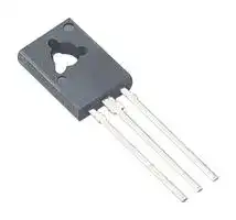
Bipolar (BJT) Single Transistor, General Purpose, PNP, 80 V, 4 A, 40 W, TO-225, Through Hole
- Manufacturer: ONSEMI
- Product type: Single Bipolar Junction Transistors - BJT
- Transistor Polarity:PNP; Collector Emitter Voltage V(br)ceo:-80V; Transition Frequency ft:2MHz; Power Dissipation Pd:40W; DC Collector Current:-4A; DC Current Gain hFE:80hFE; Transistor Case Styl
- MSL: -
- SVHC: Lead (25-Jun-2025)
- No. of Pins: 3Pins
- Product Range: -
- Qualification: -
- Power Dissipation: 40W
- Transistor Mounting: Through Hole
- Transistor Polarity: PNP
- Transition Frequency: 2MHz
- Transistor Case Style: TO-225
- DC Current Gain hFE Min: 80hFE
- Operating Temperature Max: 150°C
- Continuous Collector Current: 4A
- Collector Emitter Voltage Max: 80V
| Delivery and price | |
|---|---|
| Units per pack | 5000 |
| Price | 0.287 € |
| Current stock | 1000+ |
| Lead time | 7 days |
2N5194G, 2N5195G

## Silicon PNP Power Transistors

These devices are designed for use in power amplifier and switching circuits; excellent safe area limits.

## **Features**

## **http://onsemi.com**

- Complement to NPN 2N5191, 2N5192

**4 AMPERE POWER TRANSISTORS PNP SILICON 60 − 80 VOLTS**

• These Devices are Pb−Free and are RoHS Compliant* **POWER TRANSISTORS MAXIMUM RATINGS** (Note 1) **PNP SILICON Rating Symbol Value Unit 60 − 80 VOLTS** Collector−Emitter Voltage VCEO Vdc 2N5194G 60 COLLECTOR 2N5195G 80 2, 4 Collector−Base Voltage VCB Vdc 2N5194G 60 2N5195G 80 3 Emitter−Base Voltage VEB 5.0 Vdc BASE Collector Current IC 4.0 Adc 1 Base Current IB 1.0 Adc EMITTER Total Device Dissipation PD @ TC = 25 ° C 40 W Derate above 25 ° C 320 W/ ° C Operating and Storage Junction TJ, Tstg –65 to +150 ° C/W Temperature Range **TO−225** ~~ao~~ **CASE 77−09** Stresses exceeding those listed in the Maximum Ratings table may damage the **STYLE 1** device. If any of these limits are exceeded, device functionality should not be assumed, damage may occur and reliability may be affected. Ad 1. Indicates JEDEC registered data. 1 2 3

## **THERMAL CHARACTERISTICS**

|**THERMAL CHARACTERISTICS**||||
|---|---|---|---|
|**Characteristic**|**Symbol**|**Max**|**Unit**|
|Thermal Resistance, Junction−to−Case|R JC|3.12|°C/W|


## **MARKING DIAGRAM**

**==> picture [30 x 27] intentionally omitted <==**

**----- Start of picture text -----**<br>
YWW<br>2<br>N519xG<br>**----- End of picture text -----**<br>


Y = Year WW = Work Week 2N519x = Device Code x = 4 or 5 G = Pb−Free Package

*For additional information on our Pb−Free strategy and soldering details, please download the ON Semiconductor Soldering and Mounting Techniques Reference Manual, SOLDERRM/D.

**ORDERING INFORMATION Device Package Shipping** 2N5194G TO−225 500 Units / Bulk (Pb−Free) 2N5195G TO−225 500 Units / Bulk (Pb−Free) ~~===~~

Publication Order Number:

**1**

© Semiconductor Components Industries, LLC, 2013 **December, 2013 − Rev. 15**

**2N5194/D**

**2N5194G, 2N5195G**

## **ELECTRICAL CHARACTERISTICS** (TC = 25 � C unless otherwise noted) (Note 2)

|**ELECTRICAL CHARACTERISTICS**(TC= 25�C unless otherwise noted)|(Note 2)||||
|---|---|---|---|---|
|**Characteristic**|**Symbol**|**Min**|**Max**|**Unit**|
|**OFF CHARACTERISTICS**|||||
|Collector−Emitter Sustaining Voltage (Note 3)<br>(IC= 0.1 Adc, IB= 0)<br>2N5194G<br>2N5195G|VCEO(sus)|60<br>80|−<br>−|Vdc|
|Collector Cutoff Current<br>(VCE= 60 Vdc, IB= 0)<br>2N5194G<br>(VCE= 80 Vdc, IB= 0)<br>2N5195G|ICEO|−<br>−|1.0<br>1.0|mAdc|
|Collector Cutoff Current<br>(VCE= 60 Vdc, VBE(off)= 1.5 Vdc)<br>2N5194G<br>(VCE= 80 Vdc, VBE(off)= 1.5 Vdc)<br>2N5195G<br>(VCE= 60 Vdc, VBE(off)= 1.5 Vdc, TC= 125�C)<br>2N5194G<br>(VCE= 80 Vdc, VBE(off)= 1.5 Vdc, TC= 125�C)<br>2N5195G|ICEX|−<br>−<br>−<br>−|−0.1<br>0.1<br>2.0<br>2.0|mAdc|
|Collector Cutoff Current<br>(VCB= 60 Vdc, IE= 0)<br>2N5194G<br>(VCB= 80 Vdc, IE= 0)<br>2N5195G|ICBO|−<br>−|0.1<br>0.1|mAdc|
|Emitter Cutoff Current<br>(VBE= 5.0 Vdc, IC= 0)|IEBO|−|1.0|mAdc|
|**ON CHARACTERISTICS**|||||
|DC Current Gain (Note 3)<br>(IC= 1.5 Adc, VCE= 2.0 Vdc)<br>2N5194G<br>2N5195G<br>(IC= 4.0 Adc, VCE= 2.0 Vdc)<br>2N5194G<br>2N5195G|hFE|25<br>20<br>10<br>7.0|100<br>80<br>−<br>−|−|
|Collector−Emitter Saturation Voltage (Note 3)<br>(IC= 1.5 Adc, IB= 0.15 Adc)<br>(IC= 4.0 Adc, IB= 1.0 Adc)|VCE(sat)|−<br>−|0.6<br>1.4|Vdc|
|Base−Emitter On Voltage (Note 3)<br>(IC= 1.5 Adc, VCE= 2.0 Vdc)|VBE(on)|−|1.2|Vdc|
|**DYNAMIC CHARACTERISTICS**|||||
|Current−Gain − Bandwidth Product<br>(IC= 1.0 Adc, VCE= 10 Vdc, f = 1.0 MHz)|fT|2.0|−|MHz|


Product parametric performance is indicated in the Electrical Characteristics for the listed test conditions, unless otherwise noted. Product performance may not be indicated by the Electrical Characteristics if operated under different conditions.

2. Indicates JEDEC registered data.

3. Pulse Test: Pulse Width ≤ 300 �� s, Duty Cycle ≤ 2.0%.

**http://onsemi.com 2**

**2N5194G, 2N5195G**

**==> picture [486 x 615] intentionally omitted <==**

**----- Start of picture text -----**<br>
10<br>7.0 TJ = 150°C V CE = 2.0 V<br>5.0 V CE  = 10 V<br>3.0<br>2.0<br>1.0 25°C<br>0.7 -�55°C<br>0.5<br>0.3<br>0.2<br>0.10.004 0.007 0.01 0.02 0.03 0.05 0.1 0.2 0.3 0.5 1.0 2.0 3.0 4.0<br>IC, COLLECTOR CURRENT (AMP)<br>Figure 1. DC Current Gain<br>2.0<br>1.6<br>1.2 I C  = 10 mA 100 mA 1.0 A 3.0 A<br>0.8<br>T J  = 25°C<br>0.4<br>0<br>0.05 0.07 0.1 0.2 0.3 0.5 0.7 1.0 2.0 3.0 5.0 7.0 10 20 30 50 70 100 200 300 500<br>IB, BASE CURRENT (mA)<br>Figure 2. Collector Saturation Region<br>2.0 +�2.5<br>TJ = 25°C +�2.0 *APPLIES FOR ITJ = -�65°C to +150C/IB ≤ hFE°C @ VCE<br>1.6 +�1.5<br>+�1.0<br>1.2 +�0.5 *�VC for VCE(sat)<br>0<br>0.8 VBE(sat) @ IC/IB = 10 -�0.5<br>VBE @ VCE = 2.0 V -�1.0<br>0.4 -�1.5 �VB for VBE<br>VCE(sat) @ IC/IB = 10 -�2.0<br>0 -�2.5<br>0.005 0.01 0.02 0.03 0.05 0.1 0.2 0.3 0.5 1.0 2.0 3.0 4.0 0.005 0.01 0.020.03 0.05 0.1 0.2 0.3 0.5 1.0 2.0 3.0 4.0<br>IC, COLLECTOR CURRENT (AMP) IC, COLLECTOR CURRENT (AMP)<br>hFE, DC CURRENT GAIN (NORMALIZED)<br>VCE, COLLECTOR-EMITTER VOLTAGE (VOLTS)<br>C)°<br>VOLTAGE (VOLTS)<br>V, TEMPERATURE COEFFICIENTS (mV/<br>θ<br>**----- End of picture text -----**<br>


**Figure 3. “On” Voltage**

**Figure 4. Temperature Coefficients**

**http://onsemi.com**

**3**

**2N5194G, 2N5195G**

**==> picture [489 x 639] intentionally omitted <==**

**----- Start of picture text -----**<br>
10 [3] 10 [7]<br>V CE  = 30 Vdc VCE = 30 V<br>10 [2]<br>T J  = 150°C 10 [6]<br>IC = 10 x ICES<br>10 [1]<br>10 [5]<br>100°C<br>10 [0]<br>IC = 2 x ICES<br>IC ≈ ICES<br>10 [4]<br>10 [-1] REVERSE FORWARD<br>25°C 10 [3] (TYPICAL ICES VALUES<br>10 [-�2] OBTAINED FROM FIGURE 5)<br>ICES<br>10 [-�3] 10 [2]<br>+�0.4 +�0.3 +�0.2 +�0.1 0 -�0.1 -�0.2 -�0.3 -�0.4 -�0.5 -�0.6 20 40 60 80 100 120 140 160<br>VBE, BASE-EMITTER VOLTAGE (VOLTS) TJ, JUNCTION TEMPERATURE (°C)<br>Figure 5. Collector Cut−Off Region Figure 6. Effects of Base−Emitter Resistance<br>TURN-ON PULSE VCC RC 500<br>VBE(off) TJ = 25°C<br>Vin 0 Vin RB SCOPE<br>300<br>APPROX<br>-11 V Cjd�<<�Ceb 200<br>t1<br>APPROX +�4.0 V<br>+�9.0 V<br>t2 RB AND RC VARIED 100 Ceb<br>TO OBTAIN DESIRED<br>Vin CURRENT LEVELS Ccb<br>70<br>APPROX<br>-11 V t3 t1 ≤ 7.0 ns<br>100 < t2 < 500 �s 50<br>TURN-OFF PULSE t3 < 15 ns 0.1 0.2 0.3 0.5 1.0 2.0 3.0 5.0 10 20 30 40<br>DUTY CYCLE ≈ 2.0% VR, REVERSE VOLTAGE (VOLTS)<br>Figure 7. Switching Time Equivalent Test Circuit Figure 8. Capacitance<br>2.0 2.0<br>1.00.70.5 tr @ VCC = 30 V TICJ/I = 25B = 10°C 1.00.70.5 ts′ tIITB1CsJ′/I = t = 25 = IB = 10sB2 - 1/8 t°C f<br>0.3 0.3 tf @ VCC = 30 V<br>0.2 0.2<br>tr @ VCC = 10 V tf @ VCC = 10 V<br>0.1 0.1<br>0.07 0.07<br>0.05 0.05<br>td @ VBE(off) = 2.0 V<br>0.03 0.03<br>0.02 0.02<br>0.05 0.07 0.1 0.2 0.3 0.5 0.7 1.0 2.0 3.0 4.0 0.05 0.07 0.1 0.2 0.3 0.5 0.7 1.0 2.0 3.0 4.0<br>IC, COLLECTOR CURRENT (AMP) IC, COLLECTOR CURRENT (AMP)<br>μ<br>, COLLECTOR CURRENT (��A)<br>IC<br>RBE, EXTERNAL BASE-EMITTER RESISTANCE (OHMS)<br>CAPACITANCE (pF)<br>μ μ<br>t, TIME (��s) t, TIME (��s)<br>**----- End of picture text -----**<br>


**Figure 9. Turn−On Time**

**Figure 10. Turn−Off Time**

**http://onsemi.com**

**4**

**2N5194G, 2N5195G**

## **Note 1:**

**==> picture [234 x 170] intentionally omitted <==**

**----- Start of picture text -----**<br>
10<br>1.0 ms<br>5.0 ms<br>5.0<br>TJ = 150°C 100 �s<br>2.0 dc<br>1.0 SECONDARY BREAKDOWN LIMIT<br>THERMAL LIMIT @ TC = 25°C<br>0.5 BONDING WIRE LIMIT<br>CURVES APPLY BELOW RATED VCEO<br>0.2 2N5194<br>2N5195<br>0.1<br>1.0 2.0 5.0 10 20 50 100<br>VCE, COLLECTOR-EMITTER VOLTAGE (VOLTS)<br>IC, COLLECTOR CURRENT (AMP)<br>**----- End of picture text -----**<br>


There are two limitations on the power handling ability of a transistor; average junction temperature and second breakdown. Safe operating area curves indicate IC − VCE limits of the transistor that must be observed for reliable operation; i.e., the transistor must not be subjected to greater dissipation than the curves indicate.

The data of Figure 11 is based on TJ(pk) = 150�C. TC is variable depending on conditions. Second breakdown pulse limits are valid for duty cycles to 10% provided TJ(pk) ≤ 150�C. At high−case temperatures, thermal limitations will reduce the power that can be handled to values less than the limitations imposed by second breakdown.

**Figure 11. Rating and Thermal Data Active−Region Safe Operating Area**

**==> picture [493 x 170] intentionally omitted <==**

**----- Start of picture text -----**<br>
1.0<br>0.7<br>0.5 D = 0.5 �JC(max) = 3.12°C/W<br>0.3 0.2<br>0.2<br>0.1<br>0.1<br>0.05<br>0.07<br>0.02<br>0.05<br>0.03 0.01<br>SINGLE PULSE<br>0.02<br>0.010.01 0.02 0.03 0.05 0.1 0.2 0.3 0.5 1.0 2.0 3.0 5.0 10 20 30 50 100 200 300 500 1000<br>t, TIME OR PULSE WIDTH (ms)<br>r(t), EFFECTIVE TRANSIENT<br>THERMAL RESISTANCE (NORMALIZED)<br>**----- End of picture text -----**<br>


**Figure 12. Thermal Response**

## **DESIGN NOTE: USE OF TRANSIENT THERMAL RESISTANCE DATA**

**==> picture [184 x 153] intentionally omitted <==**

**----- Start of picture text -----**<br>
t P<br>PP PP<br>t1<br>1/f<br>t1<br>DUTY CYCLE, D = t1 f = tP<br>PEAK PULSE POWER = PP<br>**----- End of picture text -----**<br>


**Figure 13.**

A train of periodical power pulses can be represented by the model shown in Figure 13. Using the model and the device thermal response, the normalized effective transient thermal resistance of Figure 12 was calculated for various duty cycles.

To find �JC(t), multiply the value obtained from Figure 12 by the steady state value �JC.

Example:

The 2N5193 is dissipating 50 watts under the following conditions: t1 = 0.1 ms, tp = 0.5 ms. (D = 0.2).

Using Figure 12, at a pulse width of 0.1 ms and D = 0.2, the reading of r(t1, D) is 0.27.

The peak rise in junction temperature is therefore:

� T = r(t) x PP x � JC = 0.27 x 50 x 3.12 = 42.2 � C

**http://onsemi.com**

**5**

MECHANICAL CASE OUTLINE **PACKAGE DIMENSIONS**

**==> picture [472 x 503] intentionally omitted <==**

**----- Start of picture text -----**<br>
TO−225<br>CASE 77−09<br>4 ISSUE AD<br>DATE 25 MAR 2015<br>1 3<br>2 3 2 1<br>FRONT VIEW BACK VIEW<br>SCALE 1:1<br>E NOTES:<br>1. DIMENSIONING AND TOLERANCING PER<br>A1 ASME Y14.5M, 1994.<br>2. CONTROLLING DIMENSION: MILLIMETERS.<br>Q A 3. NUMBER AND SHAPE OF LUGS OPTIONAL.<br>a<br>PIN 4 MILLIMETERS<br>BACKSIDE TAB DIM MIN MAX<br>A 2.40 3.00<br>A1 1.00 1.50<br>b 0.60 0.90<br>D b2 0.51 0.88<br>P c 0.39 0.63<br>D 10.60 11.10<br>E 7.40 7.80<br>1 2 3<br>a t e 2.04 2.54<br>L 14.50 16.63<br>Jt L1 1.27 2.54<br>P 2.90 3.30<br>L1 Q 3.80 4.20<br>GENERIC<br>L<br>MARKING DIAGRAM*<br>YWW<br>XX<br>XXXXXG<br>2X b2 Y = Year<br>WW = Work Week<br>2X e XXXXX = Device Code<br>b c G = Pb−Free Package<br>*This information is generic. Please refer to<br>FRONT VIEW SIDE VIEW<br>device data sheet for actual part marking.<br>Pb−Free indicator, “G” or microdot “ ”,<br>may or may not be present.<br>STYLE 1: STYLE 2: STYLE 3: STYLE 4: STYLE 5:<br>PIN 1. EMITTER PIN 1. CATHODE PIN 1. BASE PIN 1. ANODE 1 PIN 1. MT 1<br>2., 4. COLLECTOR 2., 4. ANODE 2., 4. COLLECTOR 2., 4. ANODE 2 2., 4. MT 2<br>3. BASE 3. GATE 3. EMITTER 3. GATE 3. GATE<br>STYLE 6: STYLE 7: STYLE 8: STYLE 9: STYLE 10:<br>PIN 1. CATHODE PIN 1. MT 1 PIN 1. SOURCE PIN 1. GATE PIN 1. SOURCE<br>2., 4. GATE 2., 4. GATE 2., 4. GATE 2., 4. DRAIN 2., 4. DRAIN<br>3. ANODE 3. MT 2 3. DRAIN 3. SOURCE 3. GATE<br>**----- End of picture text -----**<br>


DATE 25 MAR 2015

Electronic versions are uncontrolled except when accessed directly from the Document Repository. **DOCUMENT NUMBER: 98ASB42049B** Printed  versions are uncontrolled  except when stamped  “CONTROLLED COPY” in red. **DESCRIPTION: TO−225 PAGE 1 OF 1** ~~re~~ ON Semiconductor and          are trademarks of Semiconductor Components Industries, LLC dba ON Semiconductor or its subsidiaries in the United States and/or other countries. ON Semiconductor reserves the right to make changes without further notice to any products herein. ON Semiconductor makes no warranty, representation or guarantee regarding the suitability of its products for any particular purpose, nor does ON Semiconductor assume any liability arising out of the application or use of any product or circuit, and specifically disclaims any and all liability, including without limitation special, consequential or incidental damages. ON Semiconductor does not convey any license under its patent rights nor the rights of others.

www.onsemi.com

© Semiconductor Components Industries, LLC, 2019

**onsemi** , , and other names, marks, and brands are registered and/or common law trademarks of Semiconductor Components Industries, LLC dba “ **onsemi** ” or its affiliates and/or subsidiaries in the United States and/or other countries. **onsemi** owns the rights to a number of patents, trademarks, copyrights, trade secrets, and other intellectual property. A listing of **onsemi’s** product/patent coverage may be accessed at www.onsemi.com/site/pdf/Patent−Marking.pdf. **onsemi** reserves the right to make changes at any time to any products or information herein, without notice. The information herein is provided “as−is” and **onsemi** makes no warranty, representation or guarantee regarding the accuracy of the information, product features, availability, functionality, or suitability of its products for any particular purpose, nor does **onsemi** assume any liability arising out of the application or use of any product or circuit, and specifically disclaims any and all liability, including without limitation special, consequential or incidental damages. Buyer is responsible for its products and applications using **onsemi** products, including compliance with all laws, regulations and safety requirements or standards, regardless of any support or applications information provided by **onsemi** . “Typical” parameters which may be provided in **onsemi** data sheets and/or specifications can and do vary in different applications and actual performance may vary over time. All operating parameters, including “Typicals” must be validated for each customer application by customer’s technical experts. **onsemi** does not convey any license under any of its intellectual property rights nor the rights of others. **onsemi** products are not designed, intended, or authorized for use as a critical component in life support systems or any FDA Class 3 medical devices or medical devices with a same or similar classification in a foreign jurisdiction or any devices intended for implantation in the human body. Should Buyer purchase or use **onsemi** products for any such unintended or unauthorized application, Buyer shall indemnify and hold **onsemi** and its officers, employees, subsidiaries, affiliates, and distributors harmless against all claims, costs, damages, and expenses, and reasonable attorney fees arising out of, directly or indirectly, any claim of personal injury or death associated with such unintended or unauthorized use, even if such claim alleges that **onsemi** was negligent regarding the design or manufacture of the part. **onsemi** is an Equal Opportunity/Affirmative Action Employer. This literature is subject to all applicable copyright laws and is not for resale in any manner.

## **PUBLICATION ORDERING INFORMATION**

**LITERATURE FULFILLMENT** : **TECHNICAL SUPPORT Email Requests to:** orderlit@onsemi.com **North American Technical Support: Europe, Middle East and Africa Technical Support:** Voice Mail: 1 800−282−9855 Toll Free USA/Canada Phone: 00421 33 790 2910 **onsemi Website:** www.onsemi.com Phone: 011 421 33 790 2910 For additional information, please contact your local Sales Representative

◊

**==> picture [232 x 43] intentionally omitted <==**
Updated at March 24, 2026
onsemi is a premier global supplier of intelligent power and sensing technologies, driving disruptive innovations across the automotive, industrial, and cloud infrastructure markets. Recognized for their commitment to sustainability and reliable supply chains, the company accelerates advancements in vehicle electrification, industrial automation, and 5G networks by solving the industry's most complex design challenges. At the core of their portfolio is an industry-leading selection of discrete semiconductors. This extensive range features thousands of high-performance bipolar transistors, single and dual MOSFETs, and a comprehensive array of diodes, including Zener, Schottky, and fast-recovery rectifiers. Engineered for superior thermal performance and energy efficiency, these foundational components are critical for demanding power conversion, switching, and signal conditioning applications. Beyond essential discretes, onsemi provides a robust suite of advanced power management and circuit protection solutions. Their lineup includes intelligent power modules, single IGBTs, and transient voltage suppression (TVS) diodes designed to safeguard sensitive circuitry. Complimented by integrated passive filters, AC/DC LED driver ICs, and specialized sub-2.4GHz RF transceivers, onsemi equips engineers with the scalable, high-quality technologies needed to build a cleaner, smarter, and more connected world.
About Novapart
Novapart is a B2B electronic component broker specialising in stock shortages and cost reduction. We source hard-to-find parts and identify compliant alternatives across a catalogue of 410,000+ components from 500+ manufacturers.
Learn more →Stock Shortage Specialist
When a component is unavailable, discontinued or has an unacceptable lead time, we tap into our network of vetted European and Asian distributors to source what you need — without compromising on quality or traceability.
Request a quote →Compliant Alternatives
We identify pin-to-pin, electrically equivalent substitutes that meet the same certifications (RoHS, AEC-Q100, REACH) as your original specification — validated against datasheets, not just part numbers. Often at a lower cost.
BOM Analysis service →