


2N4117A
JFET Transistor, -40 V, 90 µA, -1.8 V, TO-206AF, 4 Pin, 175 °C
- Manufacturer: VISHAY
- Product type: JFETs
- Breakdown Voltage Vbr:-40V; Zero Gate Voltage Drain Current Idss Min:30µA; Zero Gate Voltage Drain Current Idss Max:90µA; Gate-Source Cutoff Voltage Vgs(off) Max:-1.8V; Transistor Case Style:TO-
- MSL: -
- SVHC: No SVHC (17-Dec-2014)
- No. of Pins: 4 Pin
- Channel Type: N Channel
- Product Range: -
- Qualification: -
- Transistor Type: JFET
- Transistor Mounting: Through Hole
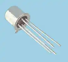
- Transistor Case Style: TO-206AF
- Operating Temperature Max: 175°C
- Gate Source Cutoff Voltage Max: -1.8V
- Gate Source Breakdown Voltage Max: -40V
- Zero Gate Voltage Drain Current Max: 90µA
- Zero Gate Voltage Drain Current Idss Min: 30µA
| Delivery and price | |
|---|---|
| Units per pack | 1000 |
| Price | 2.37 € |
| Current stock | 10+ |
| Lead time | 30 days |
**2N/PN/SST4117A Series Vishay Siliconix**

## **N-Channel JFETs**

**2N4117A PN4117A SST4117 2N4118A PN4118A SST4118 2N4119A PN4119A SST4119**

PRODUCT SUMMARY **Part Number VGS(off) (V) V(BR)GSS Min (V) gfs Min ( S) IDSS  Min ( A)** 4117 − 0.6 to − 1.8 − 40 70 30 4118 − 1 to − 3 − 40 80 80 4119 − 2 to − 6 − 40 100 200 ~~==>===~~ FEATURES BENEFITS Ultra-Low Leakage:  0.2 pA Insignificant Signal Loss/Error Voltage Very Low Current/Voltage Operation with High-Impedance Source Ultrahigh Input Impedance Low Power Consumption (Battery) Low Noise Maximum Signal Output, Low Noise

Insignificant Signal Loss/Error Voltage with High-Impedance Source Low Power Consumption (Battery) Maximum Signal Output, Low Noise High Sensitivity to Low-Level Signals

## APPLICATIONS

High-Impedance Transducer Amplifiers Smoke Detector Input Infrared Detector Amplifier Precision Test Equipment

## DESCRIPTION

The 2N/PN/SST4117A series of n-channel JFETs provide ultra-high input impedance. These devices are specified with a 1-pA limit and typically operate at 0.2 pA. This makes them perfect choices for use as high-impedance sensitive front-end amplifiers.

The hermetically sealed TO-206AF package allows full military processing per MIL-S-19500 (see Military Information). The TO-226A (TO-92) plastic package provides a low-cost option. The TO-236 (SOT-23) package provides surface-mount capability.  Both the PN and SST series are available in tape-and-reel for automated assembly (see Packaging Information).

**==> picture [96 x 162] intentionally omitted <==**

**----- Start of picture text -----**<br>
TO-206AF<br>(TO-72)<br>S C<br>1 4<br>2 3<br>D G<br>Top View<br>2N4117A<br>2N4118A<br>2N4119A<br>**----- End of picture text -----**<br>


**==> picture [40 x 17] intentionally omitted <==**

**----- Start of picture text -----**<br>
TO-226AA<br>(TO-92)<br>**----- End of picture text -----**<br>


**TO-236 (SOT-23)**

**==> picture [251 x 125] intentionally omitted <==**

**----- Start of picture text -----**<br>
D<br>1<br>D 1<br>S 2 3 G<br>S 2<br>G<br>3<br>Top View Top View<br>PN4117A SST4117 (T7)*<br>PN4118A SST4118 (T8)*<br>PN4119A SST4119 (T9)*<br>**----- End of picture text -----**<br>


*Marking Code for TO-236

For applications information see AN105.

Document Number:  70239 S-41231—Rev. G, 28-Jun-04

www.vishay.com

**1**

## **2N/PN/SST4117A Series** ~~oO~~ **Vishay Siliconix**

## ABSOLUTE MAXIMUM RATINGS

Gate-Source/Gate-Drain Voltage . . . . . . . . . . . . . . . . . . . . . . . . . . . . . . . . − 40V Lead Temperature ([1] /16” from case for 10 sec.) . . . . . . . . . . . . . . . . . . . 300 C Forward Gate Current . . . . . . . . . . . . . . . . . . . . . . . . . . . . . . . . . . . . . . . . . 50 mA Power Dissipation (case 25 C) : Storage Temperature : (2N Prefix) . . . . . . . . . . . . . . . . . . . − 65 to 175 C (2N Prefix)[a] . . . . . . . . . . . . . . . . . . . . . . 300 mW (PN, SST Prefix) . . . . . . . . . . . . . − 55 to 150 C (PN, SST Prefix)[b] . . . . . . . . . . . . . . . . 350 mW Operating Junction Temperature : Notes (2N Prefix) . . . . . . . . . . . . . . . . . . . − 55 to 175 C a. Derate 2 mW/ C above 25 C (PN, SST Prefix) . . . . . . . . . . . . . − 55 to 150 C b. Derate 2.8 mW/ C above 25 C

|SPECIFICATIONS (TA= 25 C UNLESS OTHERWISE NOTED)<br>~~a~~<br>~~eee==~~|SPECIFICATIONS (TA= 25 C UNLESS OTHERWISE NOTED)<br>~~a~~<br>~~eee==~~|SPECIFICATIONS (TA= 25 C UNLESS OTHERWISE NOTED)<br>~~a~~<br>~~eee==~~|SPECIFICATIONS (TA= 25 C UNLESS OTHERWISE NOTED)<br>~~a~~<br>~~eee==~~|SPECIFICATIONS (TA= 25 C UNLESS OTHERWISE NOTED)<br>~~a~~<br>~~eee==~~|SPECIFICATIONS (TA= 25 C UNLESS OTHERWISE NOTED)<br>~~a~~<br>~~eee==~~|SPECIFICATIONS (TA= 25 C UNLESS OTHERWISE NOTED)<br>~~a~~<br>~~eee==~~|SPECIFICATIONS (TA= 25 C UNLESS OTHERWISE NOTED)<br>~~a~~<br>~~eee==~~|SPECIFICATIONS (TA= 25 C UNLESS OTHERWISE NOTED)<br>~~a~~<br>~~eee==~~|SPECIFICATIONS (TA= 25 C UNLESS OTHERWISE NOTED)<br>~~a~~<br>~~eee==~~|SPECIFICATIONS (TA= 25 C UNLESS OTHERWISE NOTED)<br>~~a~~<br>~~eee==~~|SPECIFICATIONS (TA= 25 C UNLESS OTHERWISE NOTED)<br>~~a~~<br>~~eee==~~|
|---|---|---|---|---|---|---|---|---|---|---|---|
|**Parameter**<br>~~a~~|**Symbol**|**Test Conditions**<br>~~eee~~||**Typa**<br>~~==~~|**Limits**<br>~~p~~~~**e**~~<br>~~==~~||||||**Unit**<br>~~==~~|
||||||4117<br>~~p~~<br>~~==~~||4118<br>~~p~~~~**e**~~<br>~~==~~||4119<br>~~**e**~~<br>~~==~~|||
||||||**Min**<br>~~p~~<br>~~==~~<br>~~e~~|**Max**<br>~~p~~<br>~~==~~<br>~~e~~|**Min**<br>~~p~~~~**e**~~<br>~~==~~<br>~~e~~|**Max**<br>~~**e**~~<br>~~==~~|**Min**<br>~~**e**~~<br>~~==~~|**Max**<br>~~**e**~~<br>~~==~~||
|**Static**<br>~~eee==~~<br>~~a~~||||||||||||
|Gate-Source<br>Breakdown Voltage<br>~~a~~<br>~~po~~|V(BR)GSS<br>~~a~~<br>~~a~~|IG=−1 A , VDS= 0 V<br>~~a~~||−70<br>~~a~~|−40<br>~~a~~|~~a~~|−40<br>~~a~~|~~a~~|−40<br>~~a~~|~~a~~|**V**<br>~~a~~|
|Gate-Source Cutoff Voltage<br>~~po~~|VGS(off)<br>~~a~~|VDS= 10 V, ID= 1 nA|||−0.6|−1.8|−1|−3|−2|−6||
|Saturation Drain Current<br>~~po~~<br>~~po~~|IDSS<br>~~a~~<br>~~po~~|VDS= 10 V, VGS= 0 V<br>~~po~~||~~po~~|30<br>~~po~~|90<br>~~po~~|80<br>~~po~~|240<br>~~po~~|200<br>~~po~~|600<br>~~po~~|A<br>~~po~~|
|**G** **t**<br>**R**<br>**C**<br>**t**<br>a e everse urren|**I**<br>GSS<br>~~po~~|VGS=−20 V<br>VDS= 0 V<br>~~a~~|2N<br>~~a~~<br>~~aeeeeeeen~~<br>~~en~~|−0.2<br>~~a~~|~~a~~|−1<br>~~a~~||−1||−1<br>~~-~~|pA<br>~~-~~|
|||VGS=−20 V<br>VDS= 0 V<br>TA= 150 C<br>~~a~~<br>~~aeeeeeeen~~<br>~~ee~~||−0.4<br>~~a~~<br>~~aeeeeeeen~~<br>~~ee~~|~~a~~<br>~~aeeeeeeen~~<br>~~ee~~|−2.5<br>~~a~~<br>~~aeeeeeeen~~<br>~~eee~~|~~aeeeeeeen~~<br>~~ee~~|−2.5<br>~~aeeeeeeen~~<br>~~ee ee~~|~~aeeeeeeen~~<br>~~ee~~|−2.5<br>~~-~~<br>~~aeeeeeeen~~<br>~~ee~~|nA<br>~~-~~<br>~~aeeeeeeen~~<br>~~ee~~|
|||**VGS =−10 V**<br>VDS= 0 V<br>~~aeeeeeeen~~<br>~~ee~~<br>~~po|~~|PN<br>~~aeeeeeeen~~<br>~~en~~|−0.2<br>~~aeeeeeeen~~<br>~~ee~~|~~aeeeeeeen~~<br>~~ee~~|−1<br>~~aeeeeeeen~~<br>~~eee~~|~~aeeeeeeen~~<br>~~ee~~|−1<br>~~aeeeeeeen~~<br>~~ee ee~~|~~aeeeeeeen~~<br>~~ee~~|−1<br>~~aeeeeeeen~~<br>~~ee~~|**pA**<br>~~aeeeeeeen~~<br>~~ee~~|
||||SST<br>~~en~~<br>~~|TP~~|−0.2<br>~~ee~~<br>~~TP~~|~~ee~~<br>~~TP~~|−10<br>~~eee~~<br>~~TP~~|~~ee~~|−10<br>~~ee ee~~|~~ee~~|−10<br>~~ee~~||
|||VGS=−10 V<br>VDS= 0 V<br>TA= 100 C<br>~~ee ~~<br>~~po|~~|PN/SST<br> ~~en ~~<br>~~|TP~~|−0.03<br> ~~ee ~~<br>~~TP~~|~~ee ~~<br>~~TP~~|−2.5<br> ~~eee ~~<br>~~TP~~|~~ee~~|−2.5<br>~~ee ee~~|~~ee~~|−2.5<br>~~ee~~|nA<br>~~ee~~|
|Gate Operating Currentb<br>~~OO~~|IG<br>~~po~~<br>~~OO~~|VDG= 15 V, ID= 30 A<br>~~po | TP~~<br>~~OO~~||−0.2<br>~~TP~~<br>~~OO~~|~~TP~~<br>~~OO~~|~~TP~~<br>~~OO~~|~~OO~~|~~OO~~|~~OO~~|~~OO~~|**pA**<br>~~OO~~|
|Drain Cutoff Currentb<br>~~OO~~<br>~~pO~~|ID(off)<br>~~OO~~|VDS= 10 V, VGS=−8 V<br>~~OO~~||0.2<br>~~OO~~|~~OO~~|~~OO~~|~~OO~~|~~OO~~|~~OO~~|~~OO~~||
|Gate-Source Forward Voltageb<br>~~pO~~|VGS(F)|IG= 1 mA , VDS= 0 V||0.7|||||||V|
|**Dynamic**<br>~~pO~~<br>~~pe~~<br>~~jG~~<br>~~+}~~||||||||||||
|Common-Source<br>Forward Transconductance<br>~~jG~~<br>~~a~~|gfs<br>~~jG~~<br>~~a~~|**VDS = 10 V, VGS = 0 V**<br>f = 1 kHz<br>~~jG~~<br>~~ee~~||~~+}~~|70<br>~~+}~~|210<br>~~+}~~|80<br>~~+}~~|250|100|330|**S**|
|Common-Source<br>Output Conductance<br>~~jG~~<br>~~a~~|gos<br>~~jG~~<br>~~a~~|||~~+}~~|~~+}~~|3<br>~~+}~~|~~+}~~|5||10||
|**Common-Source**<br>Input Capacitance<br>~~jG~~<br>~~a~~<br>~~pp~~|**Ci**<br>ss<br>~~jG~~<br>~~a~~<br>~~pp~~|VDS= 10 V<br>**VGS** **= 0 V**<br>**f = 1 MHz**<br>~~jG~~<br> ~~ee~~<br>~~pp~~|2N/PN<br>~~e~~<br>~~pp~~|1.2<br>~~+}~~<br>~~pp~~|~~+}~~<br>~~pp~~|3<br>~~+}~~<br>~~pp~~|~~+}~~<br>~~pp~~|3<br>~~pp~~|~~pp~~|3<br>~~pp~~|**pF**<br>~~pp~~|
||||SST<br>~~e~~<br>~~pp~~|1.2<br>~~pp~~|~~pp~~|~~pp~~|~~pp~~|~~pp~~|~~pp~~|~~pp~~||
|**Common-Source**<br>Reverse Transfer Capacitance<br>~~a~~<br>~~pp~~<br>~~ee~~<br>~~po~~|**C**<br>rss<br>~~a ~~<br>~~pp~~<br>~~ee~~||2N/PN<br>~~e~~<br>~~pp~~|0.3<br>~~pp~~|~~pp~~|1.5<br>~~pp~~|~~pp~~|1.5<br>~~pp~~|~~pp~~|1.5<br>~~pp~~||
||||SST<br>~~pp~~|0.3<br>~~pp~~|~~pp~~|~~pp~~|~~pp~~|~~pp~~|~~pp~~|~~pp~~||
|Equivalent Input Noise Voltageb<br>~~po~~|e<br>n|VDS= 10 V, VGS= 0 V<br>f = 1 kHz||15|||||||nV⁄<br>√Hz|


- b. This parameter not registered with JEDEC.

Document Number:  70239 S-41231—Rev. G, 28-Jun-04

www.vishay.com **2**

**2N/PN/SST4117A Series Vishay Siliconix**

**==> picture [507 x 64] intentionally omitted <==**

**----- Start of picture text -----**<br>
Vishay Siliconix<br>wv<br>TYPICAL CHARACTERISTICS (TA = 25 C UNLESS OTHERWISE NOTED)<br>|<br>**----- End of picture text -----**<br>


**==> picture [481 x 611] intentionally omitted <==**

**----- Start of picture text -----**<br>
Drain Current and Transconductance<br>vs. Gate-Source Cutoff Voltage Gate Leakage Current<br>1000 300 1 nA<br>IgDSSfs @ V @ VDSDS = 10 V, V = 10 V, VGSGS = 0 V = 0 V VGS(off) =  − 2.5 V 100 mA<br>f = 1 kHz<br>800 an 240 a<br>O AL<br>100 pA<br>eh yuuanee2 TA = 125 C 10 mA IGSS @ 125 C<br>600 180<br>ee gfs .807 z 100 mA /<br>10 pA<br>OA A<br>400 120 10 mA<br>IDSS<br>200 OManne e dane 60 1 pA IGSS @ 25 Dy C L Y<br>TA = 25 C<br>0 CT E RTLE 0 0.1 pA -See| | LR]E<br>0 − 1 − 2 − 3 − 4 − 5 0 6 12 18 24 30<br>VGS(off) −  Gate-Source Cutoff Voltage (V) VDG −  Drain-Gate Voltage (V)<br>On-Resistance and Output Conductance Common-Source Forward Transconductance<br>vs. Gate-Source Cutoff Voltage vs. Drain Current<br>15 5 200<br>. PLLLLLEeZo VGS(off) =  − 2.5 V Tg LO<br>gos<br>12 e e 4 160 IAA<br>rDS<br>OCCT YT TA =  − 55 C WA<br>9 3 120 25 C<br>N CE be 125 C<br>6 NeeENC ZTEae 2 80 Aaye<br>TO REE V/A<br>3 rDS @ ID = 10 A, VGS = 0 V 1 40<br>gos @ VDS = 10 V, VGS = 0 V VDS = 10 V<br>f = 1 kHz f = 1 kHz<br>0 caeTt 0 0 Fee R<br>0 − 1 − 2 − 3 − 4 − 5 0.01 0.1 1<br>VGS(off) −  Gate-Source Cutoff Voltage (V) ID −  Drain Current (mA)<br>Output Characteristics Output Characteristics<br>100 500<br>VGS(off) =  − 0.7 V VGS(off) =  − 2.5 V<br>80 400<br>Py TT E RE VGS = 0 V Pe TaEEE<br>VGS = 0 V<br>60 SEPP − 0.1 V 300 CO P<br>eS ae FE E<br>vasnee= − 0.2 V AC T − 0.5 V<br>40 200<br>(Pao LLL − 0.3 V 7408222<br>− 1.0 V<br>(== a e − 0.4 V f o<br>20 100 − 1.5 V<br>2=— − 0.5 V ——o T<br>− 2.0 V<br>0 Zane 0 SSS<br>0 4 8 12 16 20 0 4 8 12 16 20<br>VDS −  Drain-Source Voltage (V) VDS −  Drain-Source Voltage (V)<br>g<br>A) fs<br>µ −<br> Gate Leakage<br>−<br>IG<br> Saturation Drain Current (<br>−<br> Forward Transconductance (<br>IDSS µ S)<br>)<br>gos S) µ<br>−<br> Output Conductance (<br> Drain-Source On-Resistance (k µ<br>− S)  Forward Transconductance (<br>−<br>fs<br>g<br>rDS(on)<br>A) A)<br>µ µ<br> Drain Current (  Drain Current (<br>− −<br>ID  ID<br>**----- End of picture text -----**<br>


Document Number:  70239 S-41231—Rev. G, 28-Jun-04

www.vishay.com

**3**

**2N/PN/SST4117A Series Vishay Siliconix**

## TYPICAL CHARACTERISTICS (TA = 25 C UNLESS OTHERWISE NOTED) ~~CT~~

**==> picture [480 x 608] intentionally omitted <==**

**----- Start of picture text -----**<br>
Transfer Characteristics Transconductance vs. Gate-Source Voltage<br>100 200<br>VGS(off) =  − 0.7 V VDS = 10 V VGS(off) =  − 0.7 V VDS = 10 V<br>f = 1 kHz<br>80 160<br>Po | TA =  − 55 C<br>P| | tT | te EE | TT SePR ee<br>25 C<br>60 WiAN | TA = 125 i | C ey | 120 NIN | EE||| |<br>P| | ft —L IN P t<br>40 aN 25 C 80 125 C |<br>aN | | | OT R<br>20 Pt RRA LEE| | | 40 et tePRATN |<br>− 55 C<br>e ne eee Vee<br>0 Pt] | SSN 0 Ree \eee<br>0 − 0.2 − 0.4 − 0.6 − 0.8 − 1.0 0 − 0.2 − 0.4 − 0.6 − 0.8 − 1.0<br>VGS −  Gate-Source Voltage (V) VGS −  Gate-Source Voltage (V)<br>Transfer Characteristics Transconductance vs. Gate-Source Voltage<br>500 300<br>VGS(off) =  − 2.5 V VDS = 10 V VGS(off) =  − 2.5 V VDS = 10 V<br>f = 1 kHz<br>400 240<br>Po |<br>Pt; | tT | TT Ee | Tt S NX TA =  − 55 e C Pt | oety<br>TA =  − 55 C<br>300 Na eee 180 oN 25 C Pt tt<br>25 C<br>NG tT] ty NI Pt tt<br>200 NN et | ty 120 PoNA\] | TE<br>125 C<br>PQQEE A N<br>100 125 C 60<br>N N aN<br>0 PLTNMTRAE 0 P tte| |EAEUUWTE<br>0 − 1 − 2 − 3 − 4 − 5 0 − 1 − 2 − 3 − 4 − 5<br>VGS −  Gate-Source Voltage (V) VGS −  Gate-Source Voltage (V)<br>Common-Source Input Capacitance<br>Circuit Voltage Gain vs. Drain Current vs. Gate-Source Voltage<br>100 2.0<br>gfs RL f = 1 MHz<br>AV 4 1 RLgos mail Pt | Ty<br>80 Assume VDD = 15 V, VDS = 5 V al 1.6 e ee<br>10 V mal Si tt tt ey yt<br>60 RL ID 1.2 VDS = 0 V<br>a mall Se e<br>VGS(off) =  − 0.7 V 10 V<br>40 \ 0.8 | |TT<br>N SH th SS S<br>NOSE PEE Pt tte tT ey yt<br>20 0.4<br>− 2.5 V<br>SRLSN HHIEL HEREEEEEE<br>0 i ll 0 Pitt} ttt] | fl<br>0.01 0.1 1 0 − 4 − 8 − 12 − 16 − 20<br>ID −  Drain Current (mA) VGS −  Gate-Source Voltage (V)<br>S)<br>µ<br>A)<br>µ<br> Drain Current (<br>−<br>ID<br> Forward Transconductance (<br>−<br>fs<br>g<br>S)<br>µ<br>A)<br>µ<br> Drain Current (<br>−<br>ID<br> Forward Transconductance (<br>−<br>fs<br>g<br> Voltage Gain<br>−<br>V<br>A  Input Capacitance (pF)<br>−<br>iss<br>C<br>**----- End of picture text -----**<br>


Document Number:  70239 S-41231—Rev. G, 28-Jun-04

www.vishay.com

**4**

**2N/PN/SST4117A Series Vishay Siliconix** ~~a~~

## TYPICAL CHARACTERISTICS (TA = 25 C UNLESS OTHERWISE NOTED) ~~|~~

**==> picture [502 x 408] intentionally omitted <==**

**----- Start of picture text -----**<br>
Common-Source Reverse Feedback Capacitance<br>vs. Gate-Source Voltage Equivalent Input Noise Voltage vs. Frequency<br>0.5 200<br>f = 1 MHz VDS = 10 V<br>0.4 C ASage SennenE _CREAT 160 0 1<br>0.3 120 ID = 10 mA<br>VDS = 0 V<br>AC E SCS U<br>N N ama<br>0.2 “SETTERS 80 BOHEME<br>10 V<br>TEES COE SSOCOT<br>VGS = 0 V<br>0.1 40<br>H E E Sen) SUE<br>a eg i<br>0 TEEPE Ere 0 CTP Tre 100 k<br>0 − 4 − 8 − 12 − 16 − 20 10 100 1 k 10 k<br>VGS −  Gate-Source Voltage (V) f  −  Frequency (Hz)<br>Output Conductance vs. Drain Current On-Resistance vs. Drain Current<br>2 20<br>VGS(off) =  − 0.7 V<br>VGS(off) =  − 2.5 V<br>prim At 16 a<br>TA =  − 55 C a nal | |<br>AT<br>ee n) oo<br>12<br>25 C<br>1 Ye CA<br>4 | 7<br>125 C<br>7 Ae 8 7<br>− 2.5 V<br>VDS = 10 V<br>f = 1 kHz<br>Yet i SS o o<br>Aan 4 t t<br>TA = 25 C<br>0 Coihoh 0 PT CoTt<br>0.01 0.1 1 0.01 0.1 1<br>ID −  Drain Current (mA) ID −  Drain Current (mA)<br> Noise Voltage  nV /    Hz<br>−<br>n<br> Reverse Feedback Capacitance (pF) e<br>−<br>rss<br>C<br>Ω )<br>S)<br>µ<br> Output Conductance (<br>−  Drain-Source On-Resistance (<br>os −<br>g rDS(on)<br>**----- End of picture text -----**<br>


Document Number:  70239 S-41231—Rev. G, 28-Jun-04

www.vishay.com

**5**

**Legal Disclaimer Notice**

Vishay

**==> picture [60 x 50] intentionally omitted <==**

## **Notice**

Specifications of the products displayed herein are subject to change without notice. Vishay Intertechnology, Inc., or anyone on its behalf, assumes no responsibility or liability for any errors or inaccuracies.

Information contained herein is intended to provide a product description only. No license, express or implied, by estoppel or otherwise, to any intellectual property rights is granted by this document. Except as provided in Vishay's terms and conditions of sale for such products, Vishay assumes no liability whatsoever, and disclaims any express or implied warranty, relating to sale and/or use of Vishay products including liability or warranties relating to fitness for a particular purpose, merchantability, or infringement of any patent, copyright, or other intellectual property right.

The products shown herein are not designed for use in medical, life-saving, or life-sustaining applications. Customers using or selling these products for use in such applications do so at their own risk and agree to fully indemnify Vishay for any damages resulting from such improper use or sale.

Document Number: 91000 Revision: 08-Apr-05

www.vishay.com 1
Updated at April 1, 2026
Vishay is a global leader in the manufacturing of discrete semiconductors and passive electronic components. Renowned for its exceptional quality and engineering expertise, the company produces highly reliable solutions that drive innovation across the industrial, automotive, telecommunications, and consumer electronics markets. From advanced factory automation to vehicle electrification, Vishay components provide the foundational building blocks for modern electronic design. The company's expansive portfolio is heavily focused on efficient power management, signal routing, and energy storage. Within its passive component lineup, Vishay is recognized for its extensive array of high-performance capacitors, including robust aluminium electrolytic, film, and polymer variants, alongside highly efficient power inductors. In the realm of discrete semiconductors, Vishay is a premier manufacturer of single and dual MOSFETs, as well as a vast selection of Schottky, Zener, and fast-recovery rectifier diodes designed for demanding power applications. Furthermore, Vishay delivers industry-leading circuit protection and thermal management solutions. With a broad offering of transient voltage suppressors (TVS diodes) and temperature-sensing NTC thermistors, these components are engineered to safeguard sensitive circuitry against both electrical and thermal overstress. By combining this vital mix of advanced discretes and passives, Vishay enables engineers to develop robust, space-saving, and highly resilient electronic systems.
About Novapart
Novapart is a B2B electronic component broker specialising in stock shortages and cost reduction. We source hard-to-find parts and identify compliant alternatives across a catalogue of 540,000+ components from 500+ manufacturers.
Learn more →Stock Shortage Specialist
When a component is unavailable, discontinued or has an unacceptable lead time, we tap into our network of vetted European and Asian distributors to source what you need — without compromising on quality or traceability.
Request a quote →Compliant Alternatives
We identify pin-to-pin, electrically equivalent substitutes that meet the same certifications (RoHS, AEC-Q100, REACH) as your original specification — validated against datasheets, not just part numbers. Often at a lower cost.
BOM Analysis service →