
Image not available
Illustrative purposes only

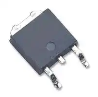
2DB1184Q-13
Bipolar (BJT) Single Transistor, PNP, 50 V, 3 A, 15 W, TO-252 (DPAK), Surface Mount
⚠️ Reference pricing provided. In case of supply shortages, we will connect you with our trusted procurement partners to ensure your project's continuity.
- Manufacturer: DIODES INC.
- Product type:
- MSL: MSL 1 - Unlimited
- SVHC: Lead (25-Jun-2025)
- No. of Pins: 3Pins
- Product Range: -
- Qualification: AEC-Q101
- Power Dissipation: 15W
- Transistor Mounting: Surface Mount
- Transistor Polarity: PNP
- Transition Frequency: 110MHz
- Transistor Case Style: TO-252 (DPAK)
- DC Current Gain hFE Min: 120hFE
- Operating Temperature Max: 150°C
- Continuous Collector Current: 3A
- Collector Emitter Voltage Max: 50V
| Delivery and price | |
|---|---|
| Units per pack | 5000 |
| Price | 0.16 € |
| Current stock | 10+ |
| Lead time | 30 days |
Datasheet

**2DB1184Q**

**50V PNP MEDIUM POWER TRANSISTOR IN TO252**

## **Features**

- BVCEO > -50V

- IC = -3A High Continuous Collector Current

- ICM = -4.5A Peak Pulse Current

- Epitaxial Planar Die Construction

- Low Collector-Emitter Saturation Voltage

- Ideal for Medium Power Switching or Amplification Applications

- **Totally Lead-Free & Fully RoHS Compliant (Notes 1 & 2)**

## **Mechanical Data**

   - Case: TO252 (DPAK)

   - Case Material:  Molded Plastic, "Green" Molding Compound. UL Flammability Classification Rating 94V-0

   - Moisture Sensitivity: Level 1 per J-STD-020

   - Terminals: Finish – Matte Tin Plated Leads, Solderable per MILSTD-202, Method 208 O **e3**

   - Weight: 0.34 grams (approximate)

- **Halogen and Antimony Free. “Green” Device (Note 3)**

- **Qualified to AEC-Q101 Standards for High Reliability**

**==> picture [57 x 8] intentionally omitted <==**

**----- Start of picture text -----**<br>
TO252 (DPAK)<br>**----- End of picture text -----**<br>


**==> picture [36 x 8] intentionally omitted <==**

**----- Start of picture text -----**<br>
Top View<br>**----- End of picture text -----**<br>


**==> picture [230 x 128] intentionally omitted <==**

**----- Start of picture text -----**<br>
C<br>C<br>B<br>B {|<br>E<br>E<br>Device Schematic Pin Out Configuration<br>Top view<br>**----- End of picture text -----**<br>


## **Ordering Information** (Note 4)

**==> picture [493 x 20] intentionally omitted <==**

**----- Start of picture text -----**<br>
||||||||
|---|---|---|---|---|---|---|
|Product|Compliance|Marking|Reel Size (inches)|Tape Width (mm)|Quantity|per Reel|
|2DB1184Q-13|AEC-Q101|2DB1184Q|13|16|2,500|

**----- End of picture text -----**<br>


- Notes: 1. No purposely added lead. Fully EU Directive 2002/95/EC (RoHS) & 2011/65/EU (RoHS 2) compliant.

   2. See http://www.diodes.com/quality/lead_free.html for more information about Diodes Incorporated’s definitions of Halogen- and Antimony-free, "Green" and Lead-free.

   3. Halogen- and Antimony-free "Green” products are defined as those which contain <900ppm bromine, <900ppm chlorine (<1500ppm total Br + Cl) and <1000ppm antimony compounds.

   4. For packaging details, go to our website at http://www.diodes.com/products/packages.html.

## **Marking Information**

**==> picture [242 x 44] intentionally omitted <==**

**----- Start of picture text -----**<br>
|||
|---|---|
|2DB1184Q = Product Type Marking Code|
|YYWW|
|= Manufacturers’ code marking|
|YYWW = Date Code Marking|
|2DB1184Q|YY = Last Digit of Year, (ex: 14 = 2014)|
|WW = Week Code 01-52|

**----- End of picture text -----**<br>


1 of 6 **www.diodes.com**

2DB1184Q Document number: DS31504 Rev. 5 - 2

May 2014 © Diodes Incorporated

**2DB1184Q**

**Absolute Maximum Ratings** (@TA = +25°C, unless otherwise specified.)

**==> picture [484 x 74] intentionally omitted <==**

**----- Start of picture text -----**<br>
|||||
|---|---|---|---|
|Characteristic|Symbol|Value|Unit|
|Collector-Base Voltage|VCBO|-60|V|
|Collector-Emitter Voltage|VCEO|-50|V|
|Emitter-Base Voltage|VEBO|-5|V|
|Continuous Collector Current|IC|-3|A|
|Peak Pulse Collector Current|ICM|-4.5|A|

**----- End of picture text -----**<br>


**Thermal Characteristics** (@TA = +25°C, unless otherwise specified.)

**==> picture [486 x 72] intentionally omitted <==**

**----- Start of picture text -----**<br>
||||||
|---|---|---|---|---|
|Characteristic|Symbol|Value|Unit|
|Power Dissipation|(Note 5)|PD|1.2|W|
|Power Dissipation @TL = +25°C|(Note 6)|PD|15|W|
|Thermal Resistance, Junction to Lead|(Note 5)|RθJA|104|°C/W|
|Thermal Resistance, Junction to Ambient|(Note 6)|RθJL|8.3|°C/W|
|Operating and Storage Temperature Range|TJ, TSTG|-55 to +150|°C|

**----- End of picture text -----**<br>


## **ESD Ratings** (Note 7)

**==> picture [513 x 33] intentionally omitted <==**

**----- Start of picture text -----**<br>
||||||
|---|---|---|---|---|
|Characteristic|Symbol|Value|Unit|JEDEC Class|
|Electrostatic Discharge - Human Body Model|ESD HBM|4000|V|3A|
|Electrostatic Discharge - Machine Model|ESD MM|400|V|C|

**----- End of picture text -----**<br>


Note: 5. For a device mounted with the exposed collector pad on minimum recommended pad (MRP) layout 1oz copper that is on a single-sided 1.6mm FR4 PCB; device is measured under still air conditions whilst operating in a steady-state.

6. Thermal resistance from junction to solder-point (on the exposed collector pad).

7. Refer to JEDEC specification JESD22-A114 and JESD22-A115.

## **Thermal Characteristics**

**==> picture [400 x 212] intentionally omitted <==**

**----- Start of picture text -----**<br>
1 SSEEESS SS ES eS SS SSSn ll<br>iii D = 0.7 saeSSS<br>D = 0.5<br>TTTNE oaTT TT<br>D = 0.3<br>0.1 (IMCHIRDUMEIneee-  ARsA eee aeemereeo e eaeAPAallin? S|TTT TUTTI<br>D = 0.1<br>ee cl agpoPEIoe a<br>TT CAATNe<br>D = 0.05 D = 0.9<br>AT CEE<br>Mee Bt RθJA(t) = r(t) * RθJA Cone<br>D = 0.02 RθJA = 110°C/W<br>HHI HIT TTT<br>eee .<br>0.01<br>CllPT D = 0.01  Tr TAA‘ire P(pk) t 1 MaPIrr)<br>a D = 0.005  a A | t 2 >| PEee<br>FyOrBIE TJ - TA = P  *  RθJA(t) CAPTPE TET<br>Duty Cycle, D = t 1 /t 2<br>D = Single Pulse<br>0.001<br>0.00001 0.0001 0.001 0.01 0.1 1 10 100 1,000 10,000<br>t1, PULSE DURATION TIME (s)<br>Figure 1 Transient Thermal Response<br>r(t), TRANSIENT THERMAL RESISTANCE<br>**----- End of picture text -----**<br>


2 of 6

2DB1184Q Document number: DS31504 Rev. 5 - 2

May 2014 © Diodes Incorporated

**www.diodes.com**

**2DB1184Q**

**Electrical Characteristics** (@TA = +25°C, unless otherwise specified.)

**==> picture [522 x 522] intentionally omitted <==**

**----- Start of picture text -----**<br>
|||||||||||||||
|---|---|---|---|---|---|---|---|---|---|---|---|---|---|
|Pf|Characteristic|Symbol|Min|Typ|Max|Unit|Test Condition|
|OFF CHARACTERISTICS (Note 8)|
|Collector-Base Breakdown Voltage|BVCBO|-60|—|—|V|IC = -50µA, IE = 0|
|TTT|EEEff|
|Collector-Emitter Breakdown Voltage|BVCEO|-50|—|—|V|IC = -1mA, IB = 0|
|a|Emitter-Base Breakdown Voltage|BVEBO|-5|—|—|V|IE = -50µA, IC = 0|
|I|Collector Cutoff Current|I|II|CBO|(OR|—|OO|—|(I|-1|(OO|µA|VCB = -40V, IE = 0|
|I|Emitter Cutoff Current|Rn|IEBO|(IID|—|I|—|(ID|-1|µA|I|VEB = - 4V, IC = 0|
|ON CHARACTERISTICS (Note 8)|
|ee|Collector-Emitter Saturation Voltage|VCE(sat)|—|—|-1|V|IC = -2A, IB = -0.2A|
|I|Base-Emitter Saturation Voltage|(RN|VBE(sat)|GO|—|(I|—|(I|-1.2|V|IC = -1.5A, IB = -0.15A|
|I|DC Current Gain|I|hFE|(I|120|OI|—|(ID|270|I|—|VCE = -3V, IC = -0.5A|
|SMALL SIGNAL CHARACTERISTICS|
|VCE = -5V, IC = -0.1A,|
|OO|Current Gain-Bandwidth Product|fT|—|110|—|MHz|f = 30MHz|
|I|Output Capacitance|(I|Cobo|OI|—|(O(N|26|—|pF|I|VCB = -10V, f = 1MHz|
|Turn-On Time|ton|—|109|—|ns|
|Delay Time|td|—|60|—|ns|
|I|Rise Time|ID|tr|UII|—|I|49|I|—|ns|VICCCC = 150mA  = 30V|
|I|Turn-Off Time|toff|I|—|I|280|I|—|ns|IB1|= - IB2|= 15mA|
|nn|Storage Time|GR|ts|OID|—|OU|246|I|—|ns|
|SSeSnr|Fall Time|t|nD|f|RO|—|ID|34|—|ns|
|Note:|8.  Measured under pulsed conditions. Pulse width ≤ 300µs. Duty cycle ≤ 2%.|
|1,000|400|
|VCE = -3V|
|350|
|TA = 150°C|
|TT|LOM|oT|
|800|
|IB = -5mA|300|
|TA = 125°C|
|eat|em|
|600|oe|IB = -4mA|||250|Sas|TA = 85°C|
|IB = -3mA|200|
|fe|TA = 25°C|TSN|Il|
|400|
|[—|150|AAI|Lug|UOT|
|oot|Conia|
|IB = -2mA|
|100|
|200|co|TA = -55°C|A|
|fy|too|IB = -1mA|50|aTN|
|0|ZN|0|BUT|
|0.1|1|10|0.001|0.01|0.1|1|10|
|-VCE, COLLECTOR-EMITTER VOLTAGE (V)|-IC, COLLECTOR CURRENT (A)|
|Figure 2 Typical Collector Current vs. Collector-Emitter Voltage|Figure 3 Typical DC Current Gain vs. Collector Current|

**----- End of picture text -----**<br>


3 of 6 **www.diodes.com**

2DB1184Q Document number: DS31504 Rev. 5 - 2

May 2014 © Diodes Incorporated

**2DB1184Q**

**==> picture [485 x 672] intentionally omitted <==**

**----- Start of picture text -----**<br>
0.4 1.2<br>IC/IB = 10 V CE  = -3V<br>Sigel<br>1.0 [| TAIN TTT Far<br>0.3<br>| UN a a A<br>0.8<br>| I T A = -55°C ET A Il<br>0.2 | 0.6 A<br>}/ cacti<br>TA = 25°C<br>TA = 150°C<br>TA = 125°C / 0.4 TA = 85 ° C PE Zl<br>f eee ee cl Ml<br>0.1 / TA = 25°CTA = 85°C 0.2 Tc TA = 150°C T A  = 125°C<br>BA TA = -55°C EN ek<br>0 Se a 0 eerPUI TERTTT CT T I UlATT<br>0.001 0.01 0.1 1 10 0.001 EL TTI 0.01 TEE 0.1 TET 1 TEI 10<br>-IC, COLLECTOR CURRENT (A) -IC, COLLECTOR CURRENT (A)<br>Figure 4 Typical Collector-Emitter Saturation Voltage Figure 5 Typical Base-Emitter Turn-On Voltage<br>vs. Collector Current vs. Collector Current<br>1.2 1,000<br>I C /I B  = 10 f = 1MHz<br>1.0<br>a a? al Eee<br>0.8 SH an T A  = -55°C EE Z7 All e Cibo e<br>TA = 25°C<br>0.6 seanti aeLXATT 100 PETTITTE TTT<br>ee TA = 85°C tt<br>TA = 125°C<br>0.4 ee ial + EPS<br>TA = 150°C Cobo<br>eaii||| Err<br>0.2 PAE meeeTET eeTET| TET ComiSSI<br>PAE SUE<br>0 10<br>0.001 ET ATI 0.01 TE I T 0.1 T C E T E 1 TET LETT 10 0.1 TUM 1 TTA 10 TM 100<br>-IC, COLLECTOR CURRENT (A) VR, REVERSE VOLTAGE (V)<br>Figure 6 Typical Base-Emitter Saturation Voltage Figure 7 Typical Capacitance Characteristics<br>vs. Collector Current<br>140 10<br>Pw = 100µs (mA)<br>120 V CE  = -5V<br>f = 30MHz<br>100 —| [pe te SSSCTTSSN Pw = 100ms (mA) TPR SST<br>1 Pw = 10ms (mA)<br>Pw = 1ms (mA)<br>80<br>DC (mA)<br>60 FIZ | ttl) td Feeet SST<br>BGRREREEee 0.1 aOe TNT<br>40<br>20 PTT] tty ytd PoeeSSS TA = 25°C NCEEeelSaBl<br>Single Non-repetitive Pulse<br>0 0.01<br>0 TEE 10 20 30 40 50 TT 60 70 ETT 80 90 100 0.1 De 1 TE 10 TT 100<br>IC, COLLECTOR CURRENT (mA) VCE, COLLECTOR-EMITTER VOLTAGE (V)<br>Figure 8 Typical Gain-Bandwidth Product vs. Collector Current Figure 9 Safe Operating Area (Note 3)<br>, COLLECTOR-EMITTER<br>CE(SAT) SATURATION VOLTAGE (V)<br>-V , BASE-EMITTER TURN-ON VOLTAGE (V)<br>BE(ON)<br>-V<br>CAPACITANCE (pF)<br>, BASE-EMITTER SATURATION VOLTAGE (V)<br>BE(SAT)<br>-V<br>, COLLECTOR CURRENT (A)<br>IC<br>, GAIN-BANDWIDTH PRODUCT (MHz)<br>fT<br>**----- End of picture text -----**<br>


4 of 6 **www.diodes.com**

2DB1184Q Document number: DS31504 Rev. 5 - 2

May 2014 © Diodes Incorporated

**2DB1184Q**

## **Package Outline Dimensions**

Please see AP02002 at http://www.diodes.com/datasheets/ap02002.pdf for the latest version.

**==> picture [465 x 215] intentionally omitted <==**

**----- Start of picture text -----**<br>
E -<br>* TO252 (DPAK)<br>| Dim Min  Max  Typ<br>| A  2.19 2.39 2.29<br>7H i i | |<br>| A1  0.00 0.13 0.08<br>i | | | |<br>A2  0.97 1.17 1.07  |<br>] i| b  | 0.64 0.88 0.783  | | | |<br>L4 | b2  0.76 1.14 0.95  [| | |<br>b3  5.21 5.46 5.33<br>c2  0.45 0.58 0.531<br>| D  6.00 6.20 6.10<br>rT ︵ ︶ D1  5.21  -  -<br>nan ︵ ︶ e  -  -  2.286<br>805.0 = E1 E  6.45 6.70 6.58 4.32  -  -<br>H  9.40 10.41 9.91<br>| JN ' Seating Plane L  1.40 1.78 1.59<br>! a : AI 7 1A | L3  0.88 1.27 1.08  | |<br>. 2 [7] [ARE] 74RI [L] | L4  0.64 1.02 0.83  | |<br>L_— | a  | 0°  | [|] 10°  -<br>All Dimensions in mm<br>= |<br>E<br>A<br>b3<br>7°±1°<br>c2<br>L3<br>D<br>L4 A2 H<br>e b 3x<br>b2 2x<br>GaugePlane<br>E1 D1 SeatingPlane<br>L<br>2.74REF<br>a<br>**----- End of picture text -----**<br>


## **Suggested Pad Layout**

Please see AP02001 at http://www.diodes.com/datasheets/ap02001.pdf for the latest version.

|||||||||||X<br>1<br>||X<br>1<br>|||||||
|---|---|---|---|---|---|---|---|---|---|---|---|---|---|---|---|---|
||||||||||||||||||
|||||||||||||||**Dimensions**||**Value(in mm)**|
|Y<br>2<br>Y2||Y<br>1<br>Y1|||||||||||||**C**<br>**X**<br>**X1**<br>**Y**||4.572<br>1.060<br>5.632<br>2.600|
||||||||;|||||||**Y1**||5.700|
|||||~~Y~~<br>,Y||||||C||||**Y2**||10.700|
|||||||X<br>xX|||~~=~~||||||||


5 of 6 **www.diodes.com**

2DB1184Q Document number: DS31504 Rev. 5 - 2

May 2014 © Diodes Incorporated

**2DB1184Q**

## **IMPORTANT NOTICE**

DIODES INCORPORATED MAKES NO WARRANTY OF ANY KIND, EXPRESS OR IMPLIED, WITH REGARDS TO THIS DOCUMENT, INCLUDING, BUT NOT LIMITED TO, THE IMPLIED WARRANTIES OF MERCHANTABILITY AND FITNESS FOR A PARTICULAR PURPOSE (AND THEIR EQUIVALENTS UNDER THE LAWS OF ANY JURISDICTION). Diodes Incorporated and its subsidiaries reserve the right to make modifications, enhancements, improvements, corrections or other changes without further notice to this document and any product described herein. Diodes Incorporated does not assume any liability arising out of the application or use of this document or any product described herein; neither does Diodes Incorporated convey any license under its patent or trademark rights, nor the rights of others.  Any Customer or user of this document or products described herein in such applications shall assume all risks of such use and will agree to hold Diodes Incorporated and all the companies whose products are represented on Diodes Incorporated website, harmless against all damages. Diodes Incorporated does not warrant or accept any liability whatsoever in respect of any products purchased through unauthorized sales channel. Should Customers purchase or use Diodes Incorporated products for any unintended or unauthorized application, Customers shall indemnify and hold Diodes Incorporated and its representatives harmless against all claims, damages, expenses, and attorney fees arising out of, directly or indirectly, any claim of personal injury or death associated with such unintended or unauthorized application. Products described herein may be covered by one or more United States, international or foreign patents pending.  Product names and markings noted herein may also be covered by one or more United States, international or foreign trademarks.

This document is written in English but may be translated into multiple languages for reference.  Only the English version of this document is the final and determinative format released by Diodes Incorporated.

## **LIFE SUPPORT**

Diodes Incorporated products are specifically not authorized for use as critical components in life support devices or systems without the express written approval of the Chief Executive Officer of Diodes Incorporated. As used herein: A.   Life support devices or systems are devices or systems which: 1. are intended to implant into the body, or 2. support or sustain life and whose failure to perform when properly used in accordance with instructions for use provided in the labeling can be reasonably expected to result in significant injury to the user. B.   A critical component is any component in a life support device or system whose failure to perform can be reasonably expected to cause the failure of the life support device or to affect its safety or effectiveness. Customers represent that they have all necessary expertise in the safety and regulatory ramifications of their life support devices or systems, and acknowledge and agree that they are solely responsible for all legal, regulatory and safety-related requirements concerning their products and any use of Diodes Incorporated products in such safety-critical, life support devices or systems, notwithstanding any devices- or systems-related information or support that may be provided by Diodes Incorporated.  Further, Customers must fully indemnify Diodes Incorporated and its representatives against any damages arising out of the use of Diodes Incorporated products in such safety-critical, life support devices or systems. Copyright © 2014, Diodes Incorporated **www.diodes.com**

6 of 6 **www.diodes.com**

2DB1184Q Document number: DS31504 Rev. 5 - 2

May 2014 © Diodes Incorporated
Updated at June 6, 2026
About Novapart
Novapart is a B2B electronic component broker specialising in stock shortages and cost reduction. We source hard-to-find parts and identify compliant alternatives across a catalogue of 540,000+ components from 500+ manufacturers.
Learn more →Stock Shortage Specialist
When a component is unavailable, discontinued or has an unacceptable lead time, we tap into our network of vetted European and Asian distributors to source what you need — without compromising on quality or traceability.
Request a quote →Compliant Alternatives
We identify pin-to-pin, electrically equivalent substitutes that meet the same certifications (RoHS, AEC-Q100, REACH) as your original specification — validated against datasheets, not just part numbers. Often at a lower cost.
BOM Analysis service →