
Image not available
Illustrative purposes only

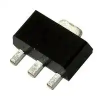
2DA1971-7
Bipolar (BJT) Single Transistor, PNP, 400 V, 500 mA, 1.5 W, SOT-89, Surface Mount
⚠️ Reference pricing provided. In case of supply shortages, we will connect you with our trusted procurement partners to ensure your project's continuity.
- Manufacturer: DIODES INC.
- Product type:
- MSL: MSL 1 - Unlimited
- SVHC: No SVHC (25-Jun-2025)
- No. of Pins: 3Pins
- Product Range: -
- Qualification: -
- Power Dissipation: 1.5W
- Transistor Mounting: Surface Mount
- Transistor Polarity: PNP
- Transition Frequency: 75MHz
- Transistor Case Style: SOT-89
- DC Current Gain hFE Min: 140hFE
- Operating Temperature Max: 150°C
- Continuous Collector Current: 500mA
- Collector Emitter Voltage Max: 400V
| Delivery and price | |
|---|---|
| Units per pack | 5000 |
| Price | 0.115 € |
| Current stock | 200+ |
| Lead time | 30 days |
Datasheet

**2DA1971**

**400V PNP HIGH VOLTAGE SWITCHING TRANSISTOR IN SOT89**

## **Features**

- BVCEO > -400V

- IC = -0.5A Continuous Collector Current

- ICM = 1A Peak Pulse Current

- High Gain Holds up hFE ≥ 140 @ IC = -100mA

- **Totally Lead-Free & Fully RoHS compliant (Notes 1 & 2)**

- **Halogen and Antimony Free. “Green” Device (Note 3)**

- **Qualified to AEC-Q101 Standards for High Reliability**

## **Mechanical Data**

- Case: SOT89

- Case material: molded plastic. “Green” molding compound. UL Flammability Rating 94V-0

- Moisture Sensitivity: Level 1 per J-STD-020

- Terminals: Finish - Matte Tin Plated Leads. Solderable per MIL-STD-202, Method 208

- Weight: 0.05 grams (Approximate)

## **Applications**

- High Voltage Switching

**==> picture [336 x 124] intentionally omitted <==**

**----- Start of picture text -----**<br>
SOT89<br>C<br>E<br>B<br>C C<br>B<br>E<br>Top View  Device symbol  Top View<br>Pin Out<br>**----- End of picture text -----**<br>


## **Ordering Information** (Note 4)

|**Ordering Informationg Information Information**(Note 4)|**Ordering Informationg Information Information**(Note 4)|**Ordering Informationg Information Information**(Note 4)|**Ordering Informationg Information Information**(Note 4)|**Ordering Informationg Information Information**(Note 4)|
|---|---|---|---|---|
||||||
|**Product**|**Marking**|**Reel size(inches)**|**Tape width(mm)**|**Quantity per reel**|
|2DA1971-7|1S2|7|12|1,000|
|2DA1971-13|1S2|13|12|2,500|


Notes: 1. No purposely added lead. Fully EU Directive 2002/95/EC (RoHS) & 2011/65/EU (RoHS 2) compliant.

   2. See http://www.diodes.com/quality/lead_free.html for more information about Diodes Incorporated’s definitions of Halogen- and Antimony-free, "Green" and Lead-free.

   3. Halogen- and Antimony-free "Green” products are defined as those which contain <900ppm bromine, <900ppm chlorine (<1500ppm total Br + Cl) and <1000ppm antimony compounds.

4. For packaging details, go to our website at http://www.diodes.com/products/packages.html.

## **Marking Information**

**==> picture [42 x 52] intentionally omitted <==**

**----- Start of picture text -----**<br>
YWW<br>1S2<br>Uo<br>Top View<br>**----- End of picture text -----**<br>


- 1S2 = Product Type Marking Code YWW = Date Code Marking

- Y = Last digit of year (ex: 1 = 2011) WW = Week code (01 – 53)

1 of 7 **www.diodes.com**

2DA1971 Document number: DS35669 Rev: 3 – 2

July 2014 © Diodes Incorporated

**2DA1971**

## **Absolute Maximum Ratings** (@TA = +25°C, unless otherwise specified.)

|**Absolute Maximum Ratingsgss** (@TA = +25°C, unless otherwise specified.)TA = +25°C, unless otherwise specified.)A = +25°C, unless otherwise specified.)= +25°C, unless otherwise specified.)|(@TA = +25°C, unless otherwise specified.)TA = +25°C, unless otherwise specified.)A = +25°C, unless otherwise specified.)= +25°C, unless otherwise specified.)pecified.)ecified.))|||
|---|---|---|---|
|**Characteristic**|**Symbol**|**Value**|**Unit**|
|Collector-Base Voltage|VCBO|-400|V|
|Collector-Emitter Voltage|VCEO|-400|V|
|Emitter-Base Voltage|VEBO|-7|V|
|Continuous Collector Current|IC|-0.5|A|
|Peak Pulse Current|ICM|-1|A|
|Base Current|IB|-250|mA|


## **Thermal Characteristics** (@TA = +25°C, unless otherwise specified.)

|**Thermal Characteristics **(@TA = +25°C, unless otherwise specified.)A = +25°C, unless otherwise specified.)= +25°C, unless otherwise specified.)|(@TA = +25°C, unless otherwise specified.)A = +25°C, unless otherwise specified.)= +25°C, unless otherwise specified.)|||
|---|---|---|---|
|**Characteristic**|**Symbol**|**Value**|**Unit**|
|Power Dissipation(Note 5)|PD|1.5|W|
|Thermal Resistance,Junction to Ambient(Note 5)|RθJA|83|°C/W|
|Thermal Resistance,Junction to Leads(Note 6)|RθJL|10.4|°C/W|
|Operatingand Storage Temperature Range|TJ,TSTG|-55 to +150|°C|


## **ESD Ratings** (Note 7)

|**ESD Ratingsgss **(Note 7)|**ESD Ratingsgss **(Note 7)|**ESD Ratingsgss **(Note 7)|**ESD Ratingsgss **(Note 7)|**ESD Ratingsgss **(Note 7)|
|---|---|---|---|---|
||||||
|**Characteristic**|**Symbol**|**Value**|**Unit**|**JEDEC Class**|
|Electrostatic Discharge - Human BodyModel|ESD HBM|8,000|V|3B|
|Electrostatic Discharge - Machine Model|ESD MM|400|V|C|


Notes: 5. For a device mounted with the exposed collector pad on 25mm x 25mm 1oz copper that is on a single-sided FR4 PCB; device is measured under still air conditions whilst operating in a steady-state.

6. Thermal resistance from junction to solder-point (on the exposed collector pad).

7. Refer to JEDEC specification JESD22-A114 and JESD22-A115.

2 of 7 **www.diodes.com**

2DA1971 Document number: DS35669 Rev: 3 – 2

July 2014 © Diodes Incorporated

**2DA1971**

## **Thermal Characteristics and Derating information**

**==> picture [508 x 408] intentionally omitted <==**

**----- Start of picture text -----**<br>
V Limit CE(sat) S511maul eee 1oz Cu; single pulse25mm x 25mm FR4 aese TA=25°C 1.5 SS\ 25mm x 25mm FR41oz Cu<br>1<br>eae a ag | | \<br>H——_4--+|_} 4 WA AANA | 1.0 IN<br>100m DC<br>po 1s ZNO OAT P| ofTNE| fd]<br>rrr TC<br>100ms<br>PT TTT 10ms ZOOSASK SN | 0.5 \Q \<br>10m<br>a 1ms 7 INE \<br>ee 100 : µs ee ee |<br>1m a ee i 0.0 N\<br>100m cee 1 10 100 ©  CODE 0 20 40 60 80 100 120 140 160<br>-VCE  Collector-Emitter Voltage (V)  Temperature (°C)<br>Safe Operating Area Derating Curve<br>80<br>TT 25mm x 25mm FR4 cccaeVVV TAI GROUUIMAUTIIPE atl a a 25mm x 25mm FR4<br>tl 1oz Cu CT 100 SCC \ 1oz Cu; single pulse<br>60 A, Vf THINS et T =25 ° C<br>A<br>TTTTi [eal] AT Seti en tee aaAaa<br>D=0.5<br>40 BUT eri | L yy)|A Uh Dy,CEU TETSU TTI TTT CT T T T TTT<br>MTIMTTTINENN'9s% VA Yl 0 10 TTILIT LITLE’'  ETT<br>r. Et tt tt<br>D=0.2 Single Pulse<br>20 a TU LrelTia Wt  ~ TeEEEOTS e reET  Nedeee ee eee eee<br>D=0.05<br>TTTT _L oe||ae || aa AlPTT ETT TTT TIMI TTT SAUTE TTT<br>D=0.1<br>0 enessetsseeonmmneat0A 1 LUI UI EITM LM aniUs<br>100µ 1m 10m 100m 1 10 100 1k 100µ 1m 10m 100m 1 10 100 1k<br>Pulse Width (s) Pulse Width (s)<br>Transient Thermal Impedance Pulse Power Dissipation<br>  Collector Current (A)<br>C<br>-I<br> Max Power Dissipation (W)<br>Thermal Resistance (°C/W)  Max Power Dissipation (W)<br>**----- End of picture text -----**<br>


3 of 7 **www.diodes.com**

2DA1971 Document number: DS35669 Rev: 3 – 2

July 2014 © Diodes Incorporated

**2DA1971**

**Electrical Characteristics** (@TA = +25°C, unless otherwise specified.)

|**Electrical Characteristics** (@TA = +25°C, unless otherwise specified.)TA = +25°C, unless otherwise specified.)A = +25°C, unless otherwise specified.)= +25°C, unless otherwise specified.)|(@TA = +25°C, unless otherwise specified.)TA = +25°C, unless otherwise specified.)A = +25°C, unless otherwise specified.)= +25°C, unless otherwise specified.)|(@TA = +25°C, unless otherwise specified.)TA = +25°C, unless otherwise specified.)A = +25°C, unless otherwise specified.)= +25°C, unless otherwise specified.)pecified.)ecified.))|(@TA = +25°C, unless otherwise specified.)TA = +25°C, unless otherwise specified.)A = +25°C, unless otherwise specified.)= +25°C, unless otherwise specified.)pecified.)ecified.))||||
|---|---|---|---|---|---|---|
|**Characteristic**<br>~~————~~|**Symbol**<br>~~————~~|**Min**<br>~~————~~|**Typ**<br>~~————~~|**Max**<br>~~————~~|**Unit**<br>~~————~~|**Test Condition**<br>~~————~~|
|Collector-Base Breakdown Voltage<br>~~————~~|BVCBO<br>~~————~~|-400<br>~~————~~|-<br>~~————~~|-<br>~~————~~|V<br>~~————~~|IC= -100µA<br>~~————~~|
|Collector-Emitter Breakdown Voltage(Note 8)<br>~~Ce~~|BVCEO<br>~~Ce~~<br>~~ff~~|-400<br>~~Ce~~<br>~~ff~~|-<br>~~Ce~~<br>~~ff~~|-<br>~~Ce~~|V<br>~~Ce~~|IC= -1mA<br>~~Ce~~|
|Emitter-Base Breakdown Voltage<br>~~Cf~~|BVEBO<br>~~Cf~~<br>~~ff~~|-7<br>~~Cf~~<br>~~ff~~|-<br>~~Cf~~<br>~~ff~~|-<br>~~Cf~~|V<br>~~Cf~~|IE= -100µA<br>~~Cf~~|
|Collector-Emitter Cut-off Current<br>~~ee~~|ICES<br>~~ff~~<br>~~ee~~|-<br>~~ff~~<br>~~ee~~|-<br>~~ff~~<br>~~ee~~|-100<br>~~ee~~|nA<br>~~ee~~|VCE= -320V<br>~~ee~~|
|Collector Cut-off Current<br>~~ee~~|ICBO<br>~~ee~~|-<br>~~ee~~|-<br>~~ee~~|-100<br>~~ee~~|nA<br>~~ee~~|VCB= -320V<br>~~ee~~|
|Emitter Cut-off Current<br>~~ee~~|IEBO<br>~~ee~~|-<br>~~ee~~|-<br>~~ee~~|-100<br>~~ee~~|nA<br>~~ee~~|VEB= -6V<br>~~ee~~|
|Static Forward Current Transfer Ratio (Note 8)<br>~~OO~~|hFE<br>~~OO~~|140<br>140<br>~~OO~~|-<br>~~OO~~|450<br>400<br>~~OO~~|-<br>~~OO~~|IC= -20mA, VCE= -5V<br>IC= -100mA,VCE= -5V<br>~~OO~~|
|Collector-Emitter saturation Voltage (Note 8)<br>~~a~~|VCE(sat)<br>~~a~~<br>~~a~~|-<br>~~a~~<br>~~a~~|-<br>~~a~~|-250<br>~~a~~|mV<br>~~a~~|IC= -100mA,IB= -10mA<br>~~a~~|
|||||-400<br>~~a~~||IC= -200mA,IB= -40mA<br>~~a~~|
|Base-Emitter saturation Voltage(Note 8)<br>~~a~~|VBE(sat)<br>~~a~~<br>~~a~~|-<br>~~a~~<br>~~a~~|-0.75<br>~~a~~|-0.9<br>~~a~~|V<br>~~a~~|IC= -100mA,IB= -10mA<br>~~a~~|
|Base-Emitter Turn-On Current(Note 8)<br>~~a~~|VBE(on)<br>~~a~~<br>~~a~~|-<br>~~a~~<br>~~a~~|-<br>~~a~~|-0.8<br>~~a~~|V<br>~~a~~|IC= -200mA,VCE= -10V<br>~~a~~|
|Transition frequency<br>~~CO~~<br>~~——~~|fT<br>~~a~~<br>~~CO~~<br>~~ff~~|-<br>~~a~~<br>~~CO~~<br>~~ff~~|75<br>~~CO~~<br>~~ff~~<br>~~re~~|-<br>~~CO~~<br>~~re~~|MHz<br>~~CO~~<br>~~re~~|IC= -50mA, VCE= -5V,<br>f = 50MHz<br>~~CO~~<br>~~re~~|
|Collector Output Capacitance<br>~~Ce~~<br>~~——~~|Cobo<br>~~Ce~~<br>~~ff~~|-<br>~~Ce~~<br>~~ff~~|19<br>~~Ce~~<br>~~ff~~<br>~~re~~|-<br>~~Ce~~<br>~~re~~|pF<br>~~Ce~~<br>~~re~~|VCB= -10V,IE= 0,f = 1MHz<br>~~Ce~~<br>~~re~~|
|DelayTime<br>~~——~~|t(d)<br>~~ff~~|-<br>~~ff~~|89<br>~~ff~~<br>~~re~~|-<br>~~re~~|ns<br>~~re~~|VCC= -200V, IC= -100mA,<br>IB1= -10mA, IB2= 20mA<br>~~re~~|
|Rise Time<br>~~——~~|t(r)<br>~~ff~~|-<br>~~ff~~|111<br>~~ff~~<br>~~re~~|-<br>~~re~~|ns<br>~~re~~||
|Storage Time<br>~~——~~<br>~~rr~~|t(s)<br>~~ff~~<br>~~rr~~|-<br>~~ff~~<br>~~rr~~|2165<br>~~ff~~<br>~~re~~<br>~~rr~~|-<br>~~re~~<br>~~rr~~|ns<br>~~re~~<br>~~rr~~||
|Fall Time<br>~~——~~<br>~~rr~~|t(f)<br>~~ff~~<br>~~rr~~|-<br>~~ff~~<br>~~rr~~|185<br>~~ff~~<br>~~re~~<br>~~rr~~|-<br>~~re~~<br>~~rr~~|ns<br>~~re~~<br>~~rr~~||


4 of 7 **www.diodes.com**

2DA1971 Document number: DS35669 Rev: 3 – 2

July 2014 © Diodes Incorporated

**2DA1971** ~~co~~

## **Typical Electrical Characteristics** (@TA = +25°C, unless otherwise specified.)

**==> picture [444 x 553] intentionally omitted <==**

**----- Start of picture text -----**<br>
1 0.5<br>Tamb=25°C yas I /I =10 TIMI<br>C B<br>I /I =50 0.4<br>C B<br>I /I =20<br>C B i YI YNy 0.3<br>CAA Ht ere Oo<br>100m I /I =10<br>Se C B 150°C<br>al 0.2<br>100°C<br>I /I =5<br>Sa C B ri 0.1 PTT La 25°C<br>-55°C<br>10m CET| ETHIE CERT ELT] OTT 0.0 oaPfftLL<br>1m 10m 100m 1 1m 10m 100m<br>- IC   Collector Current (A) - IC   Collector Current (A)<br>V  v I V  v I<br>CE(SAT) C CE(SAT) C<br>1.0<br>V =-5V<br>150°C CE<br>250 DRS 100°C iiiiiecSSIsl 0.8 | -55°C FLeo<br>200<br>SoPI OPCoIN —a|tee LLT<br>25°C<br>150 25°C 0.6<br>100 esis vet enna 100°C<br>ST=F -55°C oT 0.4 PstT Gee  aa a<br>50<br>I /I =10<br>150°C C B<br>0 ep e er [etic] ein SSSRVN a 0.2 lllear eer TI] |<br>1m 10m 100m 1 1m 10m 100m<br>- IC   Collector Current (A) - IC   Collector Current (A)<br>h  v I V  v I<br>FE C BE(SAT) C<br>1.0<br>TT TT Ee<br>0.8 -55 ° C<br>TEEN Tt<br>cement 25°C Aol<br>0.6<br>OE<br>100°C<br>0.4 get<br>setee a<br>V =-5V<br>pee TT CE<br>150°C<br>0.2 ee | |i lll |<br>1m 10m 100m<br>- IC   Collector Current (A)<br>V  v I<br>BE(ON) C<br>  (V)   (V)<br>CE(SAT) CE(SAT)<br>- V - V<br>  (V)<br>BE(SAT)<br>- V<br>Normalised Gain<br> (V)<br>BE(ON)<br>- V<br>**----- End of picture text -----**<br>


5 of 7 **www.diodes.com**

2DA1971 Document number: DS35669 Rev: 3 – 2

July 2014 © Diodes Incorporated

**2DA1971**

## **Package Outline Dimensions**

Please see AP02002 at http://www.diodes.com/datasheets/ap02002.pdf for latest version.

**==> picture [162 x 169] intentionally omitted <==**

**----- Start of picture text -----**<br>
D1<br>C<br>H<br>H<br>E<br>B1 B L<br>Cod: e<br>8° (4X)<br>A<br>Led<br>D<br>R0.200<br>1<br>**----- End of picture text -----**<br>


|**SOT89**|**SOT89**|**SOT89**|
|---|---|---|
|**Dim**|**Min**|**Max**|
|**A**|1.40|1.60|
|**B**|0.44|0.62|
|**B1**|0.35|0.54|
|**C**|0.35|0.44|
|**D**|4.40|4.60|
|**D1**|1.62|1.83|
|**E**|2.29|2.60|
|**e**|1.50 Typ||
|**H**|3.94|4.25|
|**H1**|2.63|2.93|
|**L**|0.89|1.20|
|0.89<br>1.20<br>**All Dimensions in mm**|||


## **Suggested Pad Layout**

Please see AP02001 at http://www.diodes.com/datasheets/ap02001.pdf for the latest version.

**==> picture [104 x 115] intentionally omitted <==**

**----- Start of picture text -----**<br>
> X1<br>X2  ( 2x)<br>Y1<br>Y3 Y4<br>Y Y2<br>re<br>C<br>mo<br>X (3x)<br>**----- End of picture text -----**<br>


**==> picture [104 x 94] intentionally omitted <==**

**----- Start of picture text -----**<br>
Dimensions Value (in mm)<br>X  0.900<br>X1  1.733<br>X2  0.416<br>Y  1.300<br>Y1  4.600<br>Y2  1.475<br>Y3  0.950<br>Y4  1.125<br>C  1.500<br>**----- End of picture text -----**<br>


Note: For high voltage applications, the appropriate industry sector guidelines should be considered with regards to creepage and clearance distances between device Terminals and PCB tracking.

6 of 7 **www.diodes.com**

2DA1971 Document number: DS35669 Rev: 3 – 2

July 2014 © Diodes Incorporated

**2DA1971**

## **IMPORTANT NOTICE**

DIODES INCORPORATED MAKES NO WARRANTY OF ANY KIND, EXPRESS OR IMPLIED, WITH REGARDS TO THIS DOCUMENT, INCLUDING, BUT NOT LIMITED TO, THE IMPLIED WARRANTIES OF MERCHANTABILITY AND FITNESS FOR A PARTICULAR PURPOSE (AND THEIR EQUIVALENTS UNDER THE LAWS OF ANY JURISDICTION).

Diodes Incorporated and its subsidiaries reserve the right to make modifications, enhancements, improvements, corrections or other changes without further notice to this document and any product described herein. Diodes Incorporated does not assume any liability arising out of the application or use of this document or any product described herein; neither does Diodes Incorporated convey any license under its patent or trademark rights, nor the rights of others.  Any Customer or user of this document or products described herein in such applications shall assume all risks of such use and will agree to hold Diodes Incorporated and all the companies whose products are represented on Diodes Incorporated website, harmless against all damages.

Diodes Incorporated does not warrant or accept any liability whatsoever in respect of any products purchased through unauthorized sales channel. Should Customers purchase or use Diodes Incorporated products for any unintended or unauthorized application, Customers shall indemnify and hold Diodes Incorporated and its representatives harmless against all claims, damages, expenses, and attorney fees arising out of, directly or indirectly, any claim of personal injury or death associated with such unintended or unauthorized application.

Products described herein may be covered by one or more United States, international or foreign patents pending.  Product names and markings noted herein may also be covered by one or more United States, international or foreign trademarks.

This document is written in English but may be translated into multiple languages for reference.  Only the English version of this document is the final and determinative format released by Diodes Incorporated.

## **LIFE SUPPORT**

Diodes Incorporated products are specifically not authorized for use as critical components in life support devices or systems without the express written approval of the Chief Executive Officer of Diodes Incorporated. As used herein:

- A.   Life support devices or systems are devices or systems which:

   1. are intended to implant into the body, or

   2. support or sustain life and whose failure to perform when properly used in accordance with instructions for use provided in the labeling can be reasonably expected to result in significant injury to the user.

B.   A critical component is any component in a life support device or system whose failure to perform can be reasonably expected to cause the failure of the life support device or to affect its safety or effectiveness.

Customers represent that they have all necessary expertise in the safety and regulatory ramifications of their life support devices or systems, and acknowledge and agree that they are solely responsible for all legal, regulatory and safety-related requirements concerning their products and any use of Diodes Incorporated products in such safety-critical, life support devices or systems, notwithstanding any devices- or systems-related information or support that may be provided by Diodes Incorporated.  Further, Customers must fully indemnify Diodes Incorporated and its representatives against any damages arising out of the use of Diodes Incorporated products in such safety-critical, life support devices or systems.

Copyright © 2014, Diodes Incorporated

**www.diodes.com**

7 of 7 **www.diodes.com**

2DA1971 Document number: DS35669 Rev: 3 – 2

July 2014 © Diodes Incorporated
Updated at June 6, 2026
About Novapart
Novapart is a B2B electronic component broker specialising in stock shortages and cost reduction. We source hard-to-find parts and identify compliant alternatives across a catalogue of 540,000+ components from 500+ manufacturers.
Learn more →Stock Shortage Specialist
When a component is unavailable, discontinued or has an unacceptable lead time, we tap into our network of vetted European and Asian distributors to source what you need — without compromising on quality or traceability.
Request a quote →Compliant Alternatives
We identify pin-to-pin, electrically equivalent substitutes that meet the same certifications (RoHS, AEC-Q100, REACH) as your original specification — validated against datasheets, not just part numbers. Often at a lower cost.
BOM Analysis service →