
Image not available
Illustrative purposes only

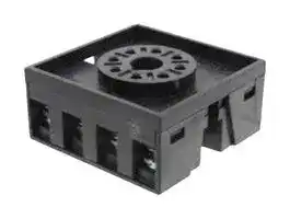
25622203
SOCKET, TIMER, PLUG-IN, 8-PIN
⚠️ Reference pricing provided. In case of supply shortages, we will connect you with our trusted procurement partners to ensure your project's continuity.
- Manufacturer: CROUZET
- Product type: Controller Accessories
- Current R; SOCKET, TIMER, PLUG-IN, 8-PIN; Current Rating:-; Product Range:Syr-line TMR48D Series
| Delivery and price | |
|---|---|
| Units per pack | 1 |
| Price | 17.1 € |
| Current stock | 10+ |
| Lead time | 30 days |
Datasheet

05-2019

## **Syr-line TMR48D Digital Timer**

## Front Panel 48x48 (1/16 DIN)

- › Large LED or LCD Screen (13.2 mm)

- › Multi-function and single-function

- › Basic & Advance configuration modes

- › Multi-range (0.05 s – 9999 h)

- › Multi-voltage (24-240 V AC/DC)

- › 1 or 2 relay outputs (Changeover)

- › Memory option in event of a break in supply

- › Lock function

- › Up or down timing

- › DIN Sized (48x48 mm) Housing

- › Compact body (63 mm long)

- › Water & Dust-proof (IP66) › 8-Pins & 11-Pins connections

_Standard Version Performance Version (MDE1) (MDA2, MDF1, GDF1, GDS2)_

## **Product Selection**

|**Product Selection**|**Product Selection**|**Product Selection**|**Product Selection**|**Product Selection**|**Product Selection**|**Product Selection**|**Product Selection**|
|---|---|---|---|---|---|---|---|
|**Type**<br>**Part Number**<br>**Function**<br>**Connections**<br>**Output**<br>**Supply Voltage**<br>**Screen**<br>**MDE1**<br>MDE1R0524U<br>A, B, C, H, D, Di<br>8-Pins<br>1 x 5A<br>24 V AC/DC<br>LCD<br>~~ee~~~~**e**~~<br>~~e~~<br>~~l rl~~||||||||
||**MDE1**|MDE1R05MVA|A, B, C, H, D, Di|8-Pins|1 x 5A|100-240 V AC/DC|LCD|
||**MDA2**|MDA2R10MV2|A|8-Pins|2 x 10A|24-240 V AC/DC|LED|
||**MDF1**|MDF1R10MV2|A, Ac, Ad, B, C, H, L, Li, D, Di|8-Pins|1 x 10A|24-240 V AC/DC|LED|
||**GDF1**|GDF1R10MV2|A, Ac, Ad, B, C, H, L, Li, D, Di|11-Pins|1 x 10A|24-240 V AC/DC|LED|
||**GDS2**|GDS2R10MV2|A, Ab, Ac, Ad, AMt, At, B, C, H, Ht, L, Li, T, W, D, Di|11-Pins|2 x 10A|24-240 V AC/DC|LED|


**==> picture [382 x 140] intentionally omitted <==**

**----- Start of picture text -----**<br>
Function<br>A:  ON-Delay Power Supply<br>E:  Multifunction E  MV2:  24-240 V AC/DC<br>F:  Multifunction F  Output Type MVA:  100-240 V AC/DC<br>S:  Multifunction S R:  Relay 24U:  24 V AC/DC<br>GD  S  2  R  10 MV2<br>Type Output Quantity Output Power<br>MD:  Digital 8-Pins 1:  1 Output 10:  10 A<br>GD:  Digital 11-Pins 2:  2 Outputs 05:  5 A<br>**----- End of picture text -----**<br>


## **Description:**

The new Syr-line Digital Timers has higher precision and many programming features with the biggest screen ever seen in the timer relays’ market and the most intuitive programming for ease to use and fast configuration

For more information about the Syr-line TMR48D Digital Timer please visit www.crouzet.com.

## **Input Specifications**

|**Input Specificationsput Specificationsut Specificationspecificationsecifications**|**Input Specificationsput Specificationsut Specificationspecificationsecifications**|**Input Specificationsput Specificationsut Specificationspecificationsecifications**|**Input Specificationsput Specificationsut Specificationspecificationsecifications**|**Input Specificationsput Specificationsut Specificationspecificationsecifications**|**Input Specificationsput Specificationsut Specificationspecificationsecifications**|
|---|---|---|---|---|---|
|**Description**<br>Rated supply voltage Un<br>**MDE1…24U**<br>24 V AC/DC<br>**MDE1…MVA**<br>100-240 V<br>AC/DC<br>**GDF1**<br>24-240 V<br>AC/DC<br>**MDF1**<br>24-240 V<br>AC/DC<br>**MDA2**<br>24-240 V<br>AC/DC<br>**GDS2**<br>24-240 V<br>AC/DC<br>~~es~~<br>~~ss~~||||||
|Voltage supply tolerance|||-15 %<br>+10 %|||
|AC supply voltage frequency|||50 / 60<br>Hz +/- 5%|||
|Galvanic isolation of supply / inputs|||N<br>o|||
|Max power consumption @ Un|||2.5 VA (VAC<br>) 1 W (VDC)|||
|Immunity to power micro cuts|||10<br>ms|||


**Timing Specifications** ~~sn~~ **Description MDE1…24U MDE1…MVA** ~~sD~~ **GDF1 MDF1 MDA2 GDS2** IEC 1812-1: 0. 001 s to 9.999 s, 0.01 s to 99.99 s, 0.1 s to 999.9 s, 1 s to 9999 s, 1 s to 99 min 59 Specified time ranges (10) s, 0.1 min to 999.9 min, 1 min to 9999min, 1 min to 99h 59 min, 0.1 h to 999.9 h, 1 h to 9999 h Minimum control pulse duration IEC 1812-1: 1 ms or 20 ms selectable Recovery time (after by de-energization) IEC 1812-1 : 120 ms Max Repeatability IEC 1812-1: ≤ ± 0.03 % ± 20 ms (VDC) / 50 ms (VAC) Setting Accuracy IEC 1812-1: ≤ ± 0.03 % ± 20 ms (VDC) / 50 ms (VAC) Temperature drift ≤ ± 0.03 % ± 20 ms (VDC) / 50 ms (VAC) Voltage drift ≤ ± 0.03 % ± 20 ms (VDC) / 50 ms (VAC)

## **Output Specifications**

|Contact arrangement<br>~~SS~~|1 CO (SPDT)<br>1 CO (SPDT)<br>2 CO (SPDT)<br>~~SS~~<br>~~eS~~|
|---|---|
|Maximum switching voltage|250 VAC / 30 VDC<br>250 VAC / 10 A resistive /<br>125 VDC / 0.3 A resistive<br>250 VAC / 10 A resistive /<br>125 VDC / 0.3 A resistive|
|Switching current rate (resistive)|NO: 5A 250 VAC / 5 A 30 VDC<br>- NC: 3A 250 VAC / 3 A 30<br>VDC<br>NO / NC: 10 A 250 VAC / 10 A<br>30 VDC<br>NO/NC: 2x10 A @ 40 °C 250 V<br>AC / 2x10 A @ 40 °C 30 VDC<br>NO / NC: 2x8 A @ 60 °C 250 V<br>AC / 2x8A @ 60 °C 30 VDC|
|Maximum switching power (resistive)|NO: 1250 VA / 150 W – NC:<br>750 VA / 90 W<br>2500 VA / 300 W<br>2 x 2500 VA / 2 x 300 W|
|Electrical life at nominal switching current<br>rate (resistive)|1x10⁵cycles NO<br>7x10⁴cycles NC<br>1x10⁵cycles (10 A 250 VAC<br>resistive)<br>1x10⁵cycles (10 A 250 VAC<br>resistive)|
|Minimum switching contact|10 mA / 12 VDC|
|Maximum rate (at max switching power)|360 cycles /hour|
|Mechanical life|10 x 106cycles|
|Dielectric strength between open contacts|1 kV / 1 min / 1 mA / 50 Hz|


Page 2 of 14

## **Insulation Specifications**

~~res~~ **Description MDE1…24U** es **MDE1…MVA** ee **GDF1 MDF1 MDA2 GDS2** Rated Insulation voltage IEC 60664-1: 300 V Insulation coordination IEC 60664-1: Overvoltage category III; pollution degree 2 Rated impulse voltage IEC 60664-1: 4 kV (1.2/50 μs) Clearance / Creepage distances IEC 60664-1: 3 mm / 3.2 mm Dielectric strength EN-61812-1: 2.5 kV / 1 min / 1 mA / 50 Hz Insulation Resistance NFC 93 050: > 500 MΩ / 250 VDC / 1min

## **General Specifications**

|**Insulation Specifications**|**Insulation Specifications**|esee||
|---|---|---|---|
|**Description**<br>**MDE1…24U**<br>Rated Insulation voltage<br>~~res~~||**MDE1…MVA**<br>**GDF1**<br>**MDF1**<br>**MDA2**<br>IEC 60664-1: 300 V<br>~~res~~<br>esee|**GDS2**<br>~~res~~|
|Insulation coordination||IEC 60664-1: Overvoltage category III; pollution degree 2||
|Rated impulse voltage||IEC 60664-1: 4 kV (1.2/50 μs)||
|Clearance / Creepage distances||IEC 60664-1: 3 mm / 3.2 mm||
|Dielectric strength||EN-61812-1: 2.5 kV / 1 min / 1 mA / 50 Hz||
|Insulation Resistance||NFC 93 050: > 500 MΩ / 250 VDC / 1min||
|**General Specifications**<br>**Description**<br>**MDE1…24U**<br>Display<br>4 digits per<br>value<br>7 segments<br>LCD<br>~~res~~||**MDE1…MVA**<br>**GDF1**<br>**MDF1**<br>**MDA2**<br>4 digits per<br>value<br>7 segments<br>LCD<br>4 digits per<br>value<br>7 segments<br>LCD with<br>backlight<br>4 digits per<br>value<br>7 segments<br>LCD with<br>backlight<br>4 digits per<br>value<br>7 segments<br>LCD with<br>backlight<br>~~res~~<br>esee|**GDS2**<br>4 digits per<br>value<br>7 segments<br>LCD with<br>backlight<br>~~res~~|
|Memory backup||EEPROM (rewrite 1,000,000 times min, 40 years data hold min)||
|Casing||48x48 mm (1/16 DIN)||
|Mounting position||All positions||
|Mounting||Mounting Front panel, by clip<br>Mountingbase-mounted on socket||
|Housing material||UL94: enclosure plastic type V0||
|Degree of protection (Front Face)|IEC 60529: IP66 with front panel seal|||
|Degree of protection (Housing)|IEC 60529: IP20|||
|Operating temperature|IEC 60068-2: -10 °C to +60 °C|||
|Storage temperature|IEC 60068-2: -30 °C to +70 °C|||
|Humidity|IEC 60068-2-30: 93 % without condensation|||
|Vibration resistance|IEC 60068-2-6: ±0.15 mm 10 Hz - 60 Hz<br>2g60 Hz - 150 Hz|||
|Shock resistance|IEC60068-2-27: 15 gn – 11 ms, 3 x 6 axis (Output non-energized)<br>5gn – 11 ms, 3 x 6 axis(Output energized)|||
|Drop to concrete floor|IEC 60068-2-32: Height: 0.75 m|||
|Weight|Approx. 105 g (150 g with packing)|||


Page 3 of 14

## **Standards Specifications**

|**Standards Specifications**|**Standards Specifications**|
|---|---|
|**Standards Specifications**<br>**Description**<br>**MDE1…24U**<br>**MDE1…MVA**<br>**GDF1**<br>**MDF1**<br>**MDA2**<br>**GDS2**<br>EU Directives<br>2014/30/EU: EMC,<br>2014/35/EU: Low voltage<br>~~SSS~~<br>SSS SSS SSSSSSSS||
|Approvals / Marking|CE, cULus Listed Industrial Control Equipment|
|Security standard|IEC 60664-1: Insulation coordination for equipment within low-voltage systems|
||2015/863/UE: RoHS|
|Conformity with environmental directives|1907/2006: Reach|
||2012/19/UE: WEEE|
|Product standard|IEC 61812-1: Specified time relays for industrial use<br>UL 508(60947-4-1): Industrial Control Equipment(NRNT- Industrial Control Switches)|
|Immunity to electrostatic discharges|Level III Air +/-8 KV / Contact +/-6 KV|
|Immunity to radiated, radio-frequency,|IEC61000-4-3: Level III, 10 V/m (80 MHz to 1 GHz) 80% AM (1 kHz), 3 V/m (1.4 to 2 GHz)|
|electromagnetic field|80% AM(1 KHz),1 V/m(2 to 2.7 GHz)80% AM(1 KHz)|
|Immunity to rapid transient bursts|IEC 61000-4-4: Level IV, direct +/-4 kV (power supply) / capacitive coupling clamp +/-2 KV,<br>(command input and outputs)|
|Immunity to shock waves on power supply|IEC 61000-4-5: Level III, line-to-earth +/-2 kV / line-to-line +/-1 kV|
|Immunity to radiofrequency in common<br>mode|IEC 61000-4-6: Level III, 10 Vrms (0,15 to 80 MHz) 80% AM (1 kHz)|
||IEC 61000-4-11:|
||Industrial Class II, 0 % residual voltage during 1 cycle AC power ports, 70 % residual voltage|
|Immunity to voltage dips and breaks|during 25/30 cycles AC power ports, 0 % residual voltage, 250/300 cycles AC power ports.<br>Residential: 0 % residual voltage during 10 cycle AC power ports, 40 % residual voltage|
||during 10 cycles AC power ports, 70 % residual voltage during 10 cycles AC power ports, 0 %|
||residual voltage, 250/300 cycles AC power ports|
|AC/DC main port emissions|EN55022 / CISPR22 Class B<br>EN 55011 / CISPR11 Class B,Group1|
|Radiated emissions|EN55022 / CISPR22 Class B<br>EN 55011 / CISPR11 Class B,Group1|


Page 4 of 14

## **Accessories**

**==> picture [398 x 275] intentionally omitted <==**

**----- Start of picture text -----**<br>
Socket for DIN Rail or Panel  Socket for DIN Rail or Panel<br>Socket with Screw Terminal<br>Mount Mount<br>Plug-In 8-Pins Plug-In 11-Pins Plug-In 8-Pins<br>e<br>25 622 130 25 622 080 25 622 203<br>Solder Plug Solder Plug Socket with Screw Terminal<br>Plug-In 8-Pins Plug-In 11-Pins Plug-In 11-Pins<br>25 622 301 25 622 076 79 694 002<br>**----- End of picture text -----**<br>


**==> picture [510 x 201] intentionally omitted <==**

**----- Start of picture text -----**<br>
nn Dimensions in(mm) |<br>Connector socket<br>11-pin 25622080 / 8-pin 25622130 79694002: Panel-mounted<br>38 23,5 47<br>| paid Og if<br>% Fmt IL) f [eon<br>| eee ~ (gi Rae 1 q<br>Solder-connected plug:<br>25622301: 8 pin  / 25622076: 11 pin<br>**----- End of picture text -----**<br>


Page 5 of 14

**Diagrams**

**==> picture [510 x 25] intentionally omitted <==**

**----- Start of picture text -----**<br>
Le Wiring Diagrams<br>MDE1…24U MDE1…MVA<br>**----- End of picture text -----**<br>


**==> picture [26 x 8] intentionally omitted <==**

**----- Start of picture text -----**<br>
MDF1<br>**----- End of picture text -----**<br>


**GDF1**

**MDA2**

**==> picture [26 x 7] intentionally omitted <==**

**----- Start of picture text -----**<br>
GDS2<br>**----- End of picture text -----**<br>


Page 6 of 14

**==> picture [510 x 206] intentionally omitted <==**

**----- Start of picture text -----**<br>
IN) Dimensions in(mm)<br>Side View Front View<br>5.0¢.0.4mm eeostenm 13.340.25mm 48.020.imm<br>| |<br>Jo @crouzet TR48@<br>— [Qc—)] =n : [—] [48.0£0.1mm][ |]<br>co Co [\i Wi [Ip]<br>== 3 44.8 *0:10 [mm]<br>| O®®O<br>Mounting Panel Cut-Out<br>**----- End of picture text -----**<br>


Page 7 of 14

**Detailed Time Chart**

## ~~eee~~ **Function Diagrams Basic Time Chart**

**==> picture [150 x 8] intentionally omitted <==**

**----- Start of picture text -----**<br>
FUNCTION A: On-Delay (Delay on make)<br>**----- End of picture text -----**<br>


U > U _ — Start a **NOT USED** ee ns Reset R2 TIMED R1/R2 Pee SeSe **A** LSS R2 TIMED , R1/R2 ~~n~~ ee R2 INST R2 —_— T R2 INST . R2 ee ee T T T t T es en eesee FUNCTION A + Memory Option StartU **NOT USED** a eee ee ee U Reset R2 TIMED R1/R2 , —- R2 TIMED R1/R2 R2 INST R2 R2 - T R2 INST ee Ceea GOi OO CS T T t1 t2 _ im rT | FUNCTION Ab: Delayed Interval | —_ U : , U pe Start ee S Reset R1 / R2 **Ab**[R2 TIMED] R2 TIMED » R1/R2 ft] et oy yy ft R2 INST R2 R2 INST Se R2 a A T1 T2 _ Ere T1 T2 T1 t T1 t T1 T2 Py Cpeee eeeCr FUNCTION Ab + Memory Option >: U = > U ——— ———— , S 4 Start seoni Reset R2 TIMED R1/R2 R2 TIMED R1/R2 oo ————E———— R2 INST > R2 papain — R2 INST a R2 a A | T1[J] T2 —_ eert T1 T2 a T1      t1 ee t2 Py T1 t ee T1 |ee T2 _— esTt T1 ee T2 eee i FUNCTION Ac: On/Off Delay (Delay on make/break) U ——————— U Start ’ fF > 2 ee ee 5 S ee ———] , Reset tf jt tty **Ac** R2 TIMED , J R1 / R2 R2 TIMED R1 / R2 , TN R2 INST , R2 R2 INST . R2 oe | | _ re eee ee ee an Py T1 T2 ToT T1 t2 T2 GPL t1 t1 T1      t1 T1 |

Page 8 of 14

## FUNCTION Ac + Memory Option

U U Start S Reset R2 TIMED a R1 / R2 — R1 / R2 Se ee ee ee ee R2 TIMED R2 INST R2 ae R2 INST R2 as oeannnannseen T1 T2 =e =» **t2A+t2B=T2** ee T1 t2 t2A        t2B t t T1 t T1 T2 T1 “LIGA a FUNCTION Ad: Delay on Start U U Start S Reset R2 TIMED R1 / R2 R2 TIMED R1 / R2 **Ad** R2 INST R2 R2 INST R2 — T T= T t1 t1 T FUNCTION Ad + Memory Option U U Start , S oo Reset _ ——sR2 TIMED , R1 / R2 tT R2 TIMED , R1 / R2 oT— — R2 INST , R2 Lo R2 INST co, R2 ILLS CIEL Cl T T t1 t2 T — Tt - **T=t1+t2** FUNCTION At: Summation Time Relay U U | Start S en a oe > Reset 0 es ee **At**[R2 TIMED] , R1 / R2 ar R2 TIMED —— R1 / R2 R2 INST R2 R2 INST R2 » — —hm alae ann a “EL t1 t2 T=t1+t2 t1 ne t2 a T t1 ee t2 T=t1+t2 FUNCTION At + Memory Option U U Start S » nm Tre Reset R2 TIMED R1 / R2 R2 TIMED R1 / R2 ea Tre R2 INST R2 R2 INST R2 > —taee , oe T=t1+t2 t1 t2 T=t1+t2 t1 t2 t1 t2 t1 t2 Tht TE,oe? UE

**==> picture [44 x 22] intentionally omitted <==**

**----- Start of picture text -----**<br>
Ad<br>**----- End of picture text -----**<br>


Page 9 of 14

FUNCTION AMt: On-Delay (Delay on make, Total memory: one delay)

**==> picture [476 x 541] intentionally omitted <==**

**----- Start of picture text -----**<br>
make, Total memory: one delay) > U —_—<br>Start  NOT USED<br>U<br>Reset<br>R2 TIMED R1 / R2<br>R2 TIMED > R1 / R2  NN eSee<br>R2 INST b R2 ee<br>R2<br>R2 INST es a A<br>T=t1+t2 t1 t2<br>t1  t2  T<br>T=t1+t2<br>FUNCTION B: One-Shot<br>U<br>U<br>7—_________—_—_™ > Start eee ae ee a ee |<br>S<br>|} |<br>, Lag ——_—_—_| ye Reset  || | | |_|<br>B  R2 TIMED , R1 / R2 tee ——}- R2 TIMED R1 / R2 a ee eee<br>R2 INST  R2<br>, a R2 INST      R2 ee<br>T<br>Ro —_ » | T Se Po T  Ey t  ee LL t  eeLg T ee<br>FUNCTION B + Memory Option<br>U<br>U<br>, oe OO> Start —————_—_—_—==a a<br>> S ——E<br>Reset<br>— ee sOOO<br>R2 TIMED , R1 / R2 —_—ESE R2 TIMED » R1 / R2 aOe ee OeGG Oe<br>R2 INST Y R2 Te T  bo R2 INST » T=t1+t2 R2 2.eea T t t1 t2 T . oo T<br>—— GL<br>FUNCTION C: Off-Delay (Delay on break)<br>U<br>U<br>Start<br>S<br>Reset<br>> St _ Soe ee ee eee<br>C  R2 TIMED R1 / R2 yy | 7 i R2 TIMED R1 / R2 Cm el _|<br>R2 INST  R2<br>» lee R2 INST      , R2 oe<br>T<br>T t  t  T<br>_, eee Bee ee<br>FUNCTION C + Memory Option<br>U<br>U<br>oe es Start a oe ee<br>S<br>, a alae ee<br>Reset<br>R2 TIMED » R1 / R2 {eeeP|rf| — — R2 TIMED >» R1 / R2R2 OePOE; || Ato)Oe es GG ooOGG<br>R2 INST > R2 ttt | R2 INST » OPee Pee<br>_ so T T=t1+t2 [|| T ptf t ppp tp t1 PT t2 PT]  tf t T<br>**----- End of picture text -----**<br>


**==> picture [37 x 15] intentionally omitted <==**

**----- Start of picture text -----**<br>
AMt<br>**----- End of picture text -----**<br>


Page 10 of 14

**==> picture [81 x 7] intentionally omitted <==**

**----- Start of picture text -----**<br>
FUNCTION H: Interval<br>**----- End of picture text -----**<br>


## **H**

**==> picture [438 x 200] intentionally omitted <==**

**----- Start of picture text -----**<br>
_ U<br>U -<br>oT Start  NOT USED<br>R2 TIMED R1 / R2<br>Reset<br>R2 INST » R2 R2 TIMED R1 / R2  _ aeeeee<br>T R2 a<br>R2 INST a T  t  a T  t  _ — T —|J<br>>" —+ +»! UL, | [—___,!]<br>FUNCTION H + Memory Option<br>> U<br>U<br>Start NOT USED<br>R2 TIMED — R1 / R2 Pt ,<br>— > Reset<br>R2 INST     ee R2 4eea R2 TIMED , R1 / R2<br>| T  R2 INST     , R2<br>T t T t1 t2<br>**----- End of picture text -----**<br>


**==> picture [114 x 8] intentionally omitted <==**

**----- Start of picture text -----**<br>
FUNCTION H + Memory Option<br>**----- End of picture text -----**<br>


FUNCTION Ht: interval summation time relay

**==> picture [558 x 320] intentionally omitted <==**

**----- Start of picture text -----**<br>
> U Po<br>U<br>Start<br>ee S<br>, Reset tp —}|_| [|__|]<br>Ht  [R2 TIMED] yn R1 / R2 | R2 TIMED R1 / R2  a ee|__|<br>R2 INST R2<br>> — fms R2 INST , R2 ee<br>T=t1+t2 t1  — t2 T=t1+t2  t1 = t2  T t1  t2<br>FUNCTION Ht + Memory Option<br>> U 7 EL es ee<br>U<br>Start eeft<br>— , tet<br>S<br>a  Reset ee Oe aee<br>» }}—_}fi] {|_| {| ___|_<br>R2 TIMED R1 / R2<br>> R2 TIMED , R1 / R2<br>R2 INST ee R2  TTPee R2 INST , R2 = = =—SE _ine "1 - |_|<br>t1  t2<br>T=t1+t2 T=t1+t2  t1  t2 t1  t2 t1  t2<br>= ey tes oe<br>FUNCTION L: Recycler (OFF Start)<br>U<br>U - .<br>Start NOT USED<br>R2 TIMED Ce R1 / R2  enTT Reset ee<br>L R2 INST » R2 R2 TIMED Oe R1 / R2<br>Py T1  T2  T1  T2 R2 a a a<br>R2 INST<br>T1  T2  T1  T2  T1  T1  T2  T1  T1<br>PPP ey<br>**----- End of picture text -----**<br>


Page 11 of 14

**==> picture [113 x 9] intentionally omitted <==**

**----- Start of picture text -----**<br>
FUNCTION L + Memory Option<br>**----- End of picture text -----**<br>


**==> picture [473 x 534] intentionally omitted <==**

**----- Start of picture text -----**<br>
» U 2<br>U<br>’ | > Start e NOT USED e e eee<br>R2 TIMED R1 / R2<br>Reset<br>R2<br>R2 INST R2 TIMED R1 / R2<br>naman amen ye e<br>TIE T1  T2  T1  T2 R2 | te |<br>R2 INST T1 = t1 + t2 moiee| T1  T2  ee T1  T2 t1  t2 T2  T1  | T1 t<br>| FUNCTION Li: Recycler (ON Start) |<br>—— U :<br>U<br>Start  NOT USED<br>R2 TIMED R1 / R2<br>Reset<br>P > pt —————_—_|__| _____, _|<br>R2<br>Li R2 INST R2 TIMED R1 / R2<br>T1  T2  T1  T2 R2<br>Py yy R2 INST ee err<br>poee T1   fe T2  ee T1  T2        [t ] T1  T2  T1         [t ] T1<br>FUNCTION Li + Memory Option<br>ep U<br>> U =<br>, Start NOT USED<br>R2 TIMED R1 / R2<br>Reset<br>R2 INST      R2 R2 TIMED R1 / R2<br>; . 9 eee a — a .<br>T1  T2 T1  T2<br>R2 INST ee R2 i__ae a| a a ee<br>T1 = t1 + t2 T1  T2  T1  T2 t1  t2 T2  T1  [t] T1  [t]<br>| J|J J J) L)J J) —LJ<br>FUNCTION T: On-Delay (Delay on make):  On<br>sum of times U<br>> U = , Start —— — 4<br>Reset<br>_. penne eeee<br>S<br>T  R2 TIMED  = R1 / R2 oa. R2 TIMED R1 / R2 Pe)er<br>R2 INST » R2 eT<br>R2 INST       | R2 T = t1 + t2 + t3     ee t1  ee| | t2   eee t3  _ ee ee t1  | t1  fj t2  eePf t3<br>T = t1 + t2 + t3  t1  t2  t3<br>ae. FOU LPO<br>FUNCTION T + Memory Option<br>U me<br>U<br> —— . Start  as =<br>S<br>ee ee TT Reset<br>R2 TIMED R1 / R2 R2 TIMED R1 / R2<br>, TTT ,  SS<br>R2 INST      EH R2 LL. R2 INST ee R2<br>T = t1 + t2 + t3  PCO t1  t2  t3 T = t1 + t2 + t2 = t2A + t2Bt3 t1 t2 t3 t1 t2A ae t2B t3<br>**----- End of picture text -----**<br>


## **Li**

Page 12 of 14

FUNCTION W: Timing after pulse of control contact

**==> picture [470 x 539] intentionally omitted <==**

**----- Start of picture text -----**<br>
contact U<br>U ls Start a eeon<br> Reset<br>W  R2 TIMED  R1 / R2S R2 TIMED R1 / R2<br>R2 INST       R2<br>R2 INST      R2 oe eee<br>T T t  T  t  T<br>— ey EP PE,<br>FUNCTION W + Memory Option<br>U<br>U<br>Start<br>S<br>, 0 Reset<br>R2 TIMED R1 / R2<br>yh ——} R2 TIMED mo R1 / R2 —<br>R2 INST     R2 R2 INST R2<br>a T T1 = t1 + t mi 2 T t t1 t2 | T<br>FUNCTION D: Symmetrical flashing (OFF<br>start) U<br>U Start NOT USED<br>Reset<br>R2 TIMED  R1 / R2<br>D  R2 INST , R2 tL R2 TIMED R1 / R2<br>R2<br>Ty T  T  T  tS T R2 INST<br>T T T T T T T T T1<br>FUNCTION D + Memory Option<br>U<br>U<br>Start NOT USED<br>R2 TIMED R1 / R2<br>Reset<br>R2 INST      a R2 R2 TIMED —— R1 / R2<br>T  T  T  T<br>: R2 INST SS R2<br>T = t1 + t2 eee T T T T t1 ae t2 T T T t<br>FUNCTION Di: Symmetrical flashing (ON<br>start) U<br>U Start NOT USED<br> Reset<br>| :<br>R2 TIMED  R1 / R2<br>R2 TIMED R1 / R 2<br>Di  R2 INST  ee R2  eee<br>T  T  T  T R2 INST  R2<br>Fl cy<br>T T T T t T T T t T<br>**----- End of picture text -----**<br>


Page 13 of 14

**==> picture [429 x 102] intentionally omitted <==**

**----- Start of picture text -----**<br>
FUNCTION Di + Memory Option > U _ _<br>a U 1 |<br>Start NOT USED<br>R2 TIMED R1 / R2 :<br>a a e_ » Reset —___{{_______| |<br>=<br>R2 INST  , R2 el R2 TIMED R1 / R2 ———<br>T T T T<br>ry] T ry R2 INST  EEE R2 | | EEE<br>T = t1 + t2 T T T T t1 t2 T T t T t<br>| J jf J | J J |<br>**----- End of picture text -----**<br>


## **Keys Function**

## **Set Time**

## **Check Configured Time and Function**

**Reset Time**

**Programming Mode**

Page 14 of 14

**Programming Mode**

~~Ld~~ **Programming Main Menu # Parameter Value** PASS Goo 1 **Pass** 0000 If "Lock" function is on, pass needs to be entered bAS! C_Prot 2 **Basic Prog** Enter to Basic Programming Mode AgUANnRLED_Prot 3 **Advanced Prog** Enter to Advanced Programming Mode CESE 4 **Test** Enter to Test Mode ~~Le~~ **Basic Prog Menu # Parameter Value** A Ab Ac Ad AMt At B C 1 **Function** HH HE L LI od dt gg Select the timing function H Ht L Li D Di T W 2 Lt mc -O.,Gg6 “ST -.---s SU --.--s[SU] ~~[OS]~~ ---.-s ----s OUT MS --m--s **Time Range** eas.em totem oth em oth ooh Select the timing range ---.-m ----m --h--m ---.-h ----h Loune uP Coun 3 **Count** Up Down Select the timing count up or down 4 **Memory** Pierror Ss oFF Off on On Activate memory option (save timing after power off) 5 oUEP Ure Ei Mf€ inASk **Output 2** Timed Instantaneous Select if Out 2 works timed or instantaneous (MDA2, GDS2)

|**#**|**Parameter**|**Value**|
|---|---|---|
|1|**Input Type**<br>Select input to work with a NPN or PNP signal<br>PrmPubE<br>_ EYPE|PNP<br>NPN<br>PrP<br>nPa|
|2|**Time Change**<br>Select if a timing change will be applied during current cycle<br>(Now) or at the end of it (End)<br>ct he LHAAGE|Now<br>End<br>nou End|
|3|**Time Limit**<br>Select upper time limit<br>cifle Lite|9999<br>0000<br>$3395<br>0000|


Page 15 of 14

4 **Brightness** 100% 50% Select screen brightness SLEEP AFEEr oF F Ss iis s30s 5 **Sleep After** Off 5s 10s 30s 60s Select the time needed to turn off the screen 6 Lote oF 6: le **Lock** Off 1 2 Select security level 1 (lock configuration) or 2 (lock all) PASS oo00 6.1 **Pass** 0000 Set password for lock option dant 6.2 **Done** Indication that the lock is on GEFAULE_SEEE! nS no YES 7 **Default Settings** No Yes Reset settings to default values Sure no YES 7.1 **Sure** No Yes Confirm if reset settings to default values dont 7.2 **Done** Indication that settings have been reset

|**#**|**Parameter**|**Value**|
|---|---|---|
|1|**Out 1**<br>Turn on/off Relay Output 1<br>ouc<br>!|Off<br>On<br>or F<br>an|
|2|**Out 2**<br>Turn on/off Relay Output 2 (MDA2, GDS2)<br>our?|Off<br>On<br>oF F<br>on|
|3|**Display**<br>Turn on/off all display segments<br>di SPLAY|Off<br>On<br>or F<br>on|
|4|**Memory**<br>Test the memory of the timer<br>NenorS|Off<br>Test<br>off<br>ESE|
|4.1|**Good**<br>Indication that the memory is working properly<br>Lood||
|4.2|**Error**<br>Indication that the memory is not working properly<br>Err.||


All specifications in this document are subject to change without written notice. Actual product may differ from pictures provided in this document.

Page 16 of 14
Updated at April 10, 2026
About Novapart
Novapart is a B2B electronic component broker specialising in stock shortages and cost reduction. We source hard-to-find parts and identify compliant alternatives across a catalogue of 410,000+ components from 500+ manufacturers.
Learn more →Stock Shortage Specialist
When a component is unavailable, discontinued or has an unacceptable lead time, we tap into our network of vetted European and Asian distributors to source what you need — without compromising on quality or traceability.
Request a quote →Compliant Alternatives
We identify pin-to-pin, electrically equivalent substitutes that meet the same certifications (RoHS, AEC-Q100, REACH) as your original specification — validated against datasheets, not just part numbers. Often at a lower cost.
BOM Analysis service →