
Image not available
Illustrative purposes only

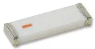
2450AT45A100E
Chip Antenna, Ceramic, 2.45 GHz, 50 Ohm, Multilayer, 9.5mm x 2mm x 1.2mm
⚠️ Reference pricing provided. In case of supply shortages, we will connect you with our trusted procurement partners to ensure your project's continuity.
- Manufacturer: JOHANSON TECHNOLOGY
- Product type: Antennas - Single Band Chip
- Centre Frequency:2.45GHz; Antenna Case Size:9.5mm x 2mm x 1.2mm; Product Range:-; SVHC:No SVHC (15-Jan-2019); Antenna Applications:Bluetooth 802.11, Cellular, DECT, GPS & WLAN; Antenna Polarisa
- SVHC: No SVHC (17-Jan-2023)
- Product Range: -
- Centre Frequency: 2.45GHz
- Antenna Case Size: 9.5mm x 2mm x 1.2mm
| Delivery and price | |
|---|---|
| Units per pack | 500 |
| Price | 0.392 € |
| Current stock | 10+ |
| Lead time | 30 days |
Datasheet

## _**"High Frequency Ceramic Solutions"**_ ee

**2.45 GHz High Gain Chip Antenna (Vertical Orientation) P/N 2450AT45A100** ~~[SSCS~~ Detail Specification: 01/05/2012 Page 1 of 10 **General Specifications Part Number** 2450AT45A100 **Input Power** 3W max. **Frequency Range** 2400 - 2500 Mhz **Impedance** 50 Ω **Peak Gain** 3.0  dBi typ. (XZ-V) **Operating Temperature** -40 to +85°C **Average Gain** 1.0  dBi typ. (XZ-V) **Reel Quanity** 1,000 **Return Loss** 9.5 dB min. ~~——~~

**==> picture [441 x 335] intentionally omitted <==**

**----- Start of picture text -----**<br>
Mechanical Dimensions Terminal Configuration<br>In mm No. Function<br>L 0.374 ± 0.008 9.50 ± 0.20 W 1 Feeding Point<br>W 0.079 ± 0.008 2.00 ± 0.20 2 NC<br>L a<br>T 0.047 +.004/-.008 1.20 +0.1/-0.2<br>— T 2 1<br>a 0.020 ± 0.012 0.50 ± 0.30<br>Mounting Considerations 1<br>Mount these devices with brown mark facing up. Units: mm<br>* Line width should be designed to provide 50Ω impedance matching characteristics.<br>1.0 1.0<br>10.5 10.5<br>GND 7.5 GND 7.5<br>*<br>* 1.8 * 1.8<br>1.5pF<br>3.9nH<br>GND GND<br>a) Without Matching Circuit (moderate bandwidth) b) With Matching Circuit* (wide bandwidth)<br>*<br>matching circuit and component values will depend and<br>EVB p/n: vary on PCB layout, thickness, material, etc.<br>2450AT45A100-EB1SMA JTI P/N for Matching Circuit:<br>**----- End of picture text -----**<br>


Mount these devices with brown mark facing up. Units: mm

* Line width should be designed to provide 50Ω impedance matching characteristics.

**JTI P/N for Matching Circuit: Cap (1.5pF): 500R07S1R5BV4T Inductor (3.9nH): L-07C3N9SV6T**

## **www.johansontechnology.com**

4001 Calle Tecate • Camarillo, CA 93012 • TEL 805.389.1166 FAX 805.389.1821 2012 Johanson Technology, Inc.  All Rights Reserved

Johanson Technology, Inc. reserves the right to make design changes without notice. All sales are subject to Johanson Technology, Inc. terms and conditions.

## _**"High Frequency Ceramic Solutions"**_

## **2.45 GHz High Gain Chip Antenna (Vertical Orientation) P/N 2450AT45A100** Detail Specification: 01/05/2012 Page 2 of 10

## **Typical Electrical Characteristics (T=25[o] C)**

**==> picture [411 x 140] intentionally omitted <==**

**----- Start of picture text -----**<br>
Test Board<br>EVB p/n: ) 40mm 12 mm<br>2450AT45A100-EB1SMA *@)O0(e) (e)) e) (e) (e) ) (e) (0) (0) (0) (0) (0) (0) (0) (0) (0) (0) (0) le) feO 50Ω Feed<br>. GND O oO000000000 Line<br>20mm :; . O i = = j =:|<br>0O () 0 (J}O 990000000OO Antenna<br>Ground 19mm No Ground<br>Return Loss<br>**----- End of picture text -----**<br>


**==> picture [313 x 130] intentionally omitted <==**

**----- Start of picture text -----**<br>
a) Without Matching Circuit a) With Matching Circuit<br>—_ 0<br>» ff Sm)<br>* ff “10 “y<br>\ f =e ‘ ie<br>{mi ¥ wy {ma ] os: [mi : \| f<br>{dB(S(1.1))=-10.051|freq=2.305GHz '\mer” [4B(S(1,1})=-10.157|treq=2 635GHz | osa 720 | [aB(S(1,1))=-10,197theq=2.200GHz 1\/<br>or [me \w ) -30| ¥\/ \mz<br>|{req=2.440GH2[B(S(1,1))=-13.020 \freqy=<br>: - Dotnet i i AO<br>12 14 16 18 20 22 24 26 28 30 32 34 36 38 4.0 10 1.2 14 16 18 20 22 24 26<br>freq, GHz ) freq. GHz<br>**----- End of picture text -----**<br>


Johanson Technology, Inc. reserves the right to make design changes without notice. All sales are subject to Johanson Technology, Inc. terms and conditions.

## **www.johansontechnology.com**

4001 Calle Tecate • Camarillo, CA 93012 • TEL 805.389.1166 FAX 805.389.1821 2012 Johanson Technology, Inc.  All Rights Reserved

## _**"High Frequency Ceramic Solutions"**_

**==> picture [444 x 472] intentionally omitted <==**

**----- Start of picture text -----**<br>
2.45 GHz High Gain Chip Antenna (Vertical Orientation) P/N 2450AT45A100<br>Detail Specification: 01/05/2012 Page 3 of 10<br>Typical Radiation Patterns<br>) XY cut @2.45GHz<br>    Vertical<br>XY-V/XY-H<br>Z     Horizontal<br>)<br>180°<br>X<br>90°<br>270°<br>Y 0°<br>XY-cut scanning direction<br>XZ-V/XZ-H XZ cut @2.45GHz<br>Y     Vertical<br>    Horizontal<br>180°<br>X<br>90°<br>270°<br>Z 0°<br>XZ-cut scanning direction<br>)<br>YZ cut @2.45GHz<br>YZ-V/YZ-H<br>X     Vertical<br>    Horizontal<br>180°<br>Y<br>90°<br>270°<br>Z 0°<br>YZ-cut scanning direction<br>**----- End of picture text -----**<br>


Johanson Technology, Inc. reserves the right to make design changes without notice. All sales are subject to Johanson Technology, Inc. terms and conditions.

## **www.johansontechnology.com**

4001 Calle Tecate • Camarillo, CA 93012 • TEL 805.389.1166 FAX 805.389.1821 2012 Johanson Technology, Inc.  All Rights Reserved

## _**"High Frequency Ceramic Solutions"**_

## **2.45 GHz High Gain Chip Antenna (Horizontal Orientation_1) P/N 2450AT45A100** ~~Ps~~ Detail Specification: 01/05/2012 Page 4 of 10

**==> picture [449 x 463] intentionally omitted <==**

**----- Start of picture text -----**<br>
General Specifications<br>Part Number 2450AT45A100<br>Frequency Range 2400 - 2500 Mhz<br>Peak Gain 1.5  dBi typ. (XZ-V)<br>Average Gain 0.0  dBi typ. (XZ-V)<br>Return Loss 9.5 dB min.<br>Mechanical Dimensions Po Terminal Configuration<br>In mm No. Function<br>W<br>L 0.374 ± 0.008 9.50 ± 0.20 1 Feeding Point<br>W 0.079 ± 0.008 2.00 ± 0.20 2 NC<br>ee L a —<br>T 0.047 +.004/-.008 1.20 +0.1/-0.2<br>T<br>a 0.020 ± 0.012 0.50 ± 0.30 2 1<br>rs rr eoae —<br>eee —<br>Mounting Considerations 2<br>Mount these devices with brown mark facing up. Units: mm<br>* Line width should be designed to provide 50Ω impedance matching characteristics.<br>7<br>GND<br>EVB p/n:<br>2450AT45A100-EB2SMA<br>a _.<br>* 1.5<br>1.5pF<br>[al SS |<br>7.5<br>Units in mm<br>GND 1.5<br>as<br>ns<br>4.8 1.8<br>JTI P/N for Matching Circuit:<br>* Cap (1.5pF): 500R07S1R5BV4T<br>matching circuit and component values will depend on<br>PCB layout, thickness, material, etc.<br>**----- End of picture text -----**<br>


Johanson Technology, Inc. reserves the right to make design changes without notice. All sales are subject to Johanson Technology, Inc. terms and conditions.

## **www.johansontechnology.com**

4001 Calle Tecate • Camarillo, CA 93012 • TEL 805.389.1166 FAX 805.389.1821 2012 Johanson Technology, Inc.  All Rights Reserved

## _**"High Frequency Ceramic Solutions"**_

**2.45 GHz High Gain Chip Antenna (Horizontal Orientation_1) P/N 2450AT45A100** Detail Specification: 01/05/2012 Page 5 of 10

**==> picture [421 x 327] intentionally omitted <==**

**----- Start of picture text -----**<br>
Typical Electrical Characteristics (T=25 [o] C)<br>Test Board 50Ω Feed Line<br>EVB p/n:<br>40mm 7mm<br>2450AT45A100-EB2SMA<br>|<+—_>|<br>© ; ° ial<br>GND<br>20mm<br>Antenna<br>Return Loss<br>Ground 19mm No Ground<br>a) With Matching Circuit<br>0<br>=~ -10 mi m3<br>= freq=2.328GHz freqs2.567GHZz<br>a. aB(S{1,1)}=-9.984 dB(S{1,1)}=-10.012 | e<br>aw -15 ) 5 aa =<br>**----- End of picture text -----**<br>


Johanson Technology, Inc. reserves the right to make design changes without notice. All sales are subject to Johanson Technology, Inc. terms and conditions.

**www.johansontechnology.com** 4001 Calle Tecate • Camarillo, CA 93012 • TEL 805.389.1166 FAX 805.389.1821 2012 Johanson Technology, Inc.  All Rights Reserved

## _**"High Frequency Ceramic Solutions"**_

## **2.45 GHz High Gain Chip Antenna (Horizontal Orientation_1) P/N 2450AT45A100** Detail Specification: 01/05/2012 Page 6 of 10

**==> picture [394 x 483] intentionally omitted <==**

**----- Start of picture text -----**<br>
Typical Radiation Patterns<br>) XY cut @2.45GHz<br>    Vertical<br>XY-V/XY-H<br>Z     Horizontal<br>180° ) = aes<br>X<br>90°<br>270°<br>Y r= 0° P35<br>XY-cut scanning direction<br>XZ-V/XZ-H XZ cut @2.45GHz<br>Y     Vertical<br>.     Horizontal KODE<br>180°<br>| Ee e LE TEN<br>|<br>ae  oe X Asante §<br>90°<br>270°<br>~~ fue NSaE e/,<br>Z 0°<br>XZ-cut scanning direction<br>)<br>YZ cut @2.45GHz<br>YZ-V/YZ-H<br>X     Vertical<br>    Horizontal<br>180°<br>eo _i = GEER<br>T 7S, Y [REE<br>90°<br>270°<br>Ss yo ge’ ERE<br>0°<br>Z = SSB<br>YZ-cut scanning direction<br>Johanson Technology, Inc. reserves the right to make design changes without notice.<br>All sales are subject to Johanson Technology, Inc. terms and conditions.<br>**----- End of picture text -----**<br>


## **www.johansontechnology.com**

4001 Calle Tecate • Camarillo, CA 93012 • TEL 805.389.1166 FAX 805.389.1821 2012 Johanson Technology, Inc.  All Rights Reserved

## _**"High Frequency Ceramic Solutions"**_

## **2.45 GHz Antenna (Horizontal Orientation_2) P/N 2450AT45A100** ~~PO~~ Detail Specification: 01/05/2012 Page 7 of 10

**General Specifications Part Number** 2450AT45A100 **Frequency Range** 2400 - 2500 Mhz **Peak Gain** 1.3  dBi typ. (XZ-V) **Average Gain** 0.6  dBi typ. (XZ-V) **Return Loss** 9.5 dB min.

**==> picture [449 x 352] intentionally omitted <==**

**----- Start of picture text -----**<br>
Mechanical Dimensions Terminal Configuration<br>In mm No. Function<br>ee W a<br>L 0.374 ± 0.008 9.50 ± 0.20 1 Feeding Point<br>W 0.079 ± 0.008 2.00 ± 0.20 L a — 2 NC<br>T 0.047 +.004/-.008 1.20 +0.1/-0.2<br>T<br>a 0.020 ± 0.012 0.50 ± 0.30 2 1<br>-_———— St =<br>Mounting Considerations 3<br>Mount these devices with brown mark facing up. Units: mm<br>* Line width should be designed to provide 50Ω impedance matching characteristics.<br>0.5<br>10.5<br>7.5<br>GND<br>0 Ohm _|-—_,<br>1.8<br>1.5 1.5<br>* Units in mm<br>GND<br>p a m.<br>*<br>matching circuit and component values will depend on<br>PCB layout, thickness, material, etc.<br>EVB p/n:<br>2450AT45A100-EB3SMA<br>**----- End of picture text -----**<br>


Johanson Technology, Inc. reserves the right to make design changes without notice. All sales are subject to Johanson Technology, Inc. terms and conditions.

**www.johansontechnology.com**

4001 Calle Tecate • Camarillo, CA 93012 • TEL 805.389.1166 FAX 805.389.1821 2012 Johanson Technology, Inc.  All Rights Reserved

**==> picture [317 x 18] intentionally omitted <==**

**----- Start of picture text -----**<br>
"High Frequency Ceramic Solutions"<br>**----- End of picture text -----**<br>


**==> picture [516 x 366] intentionally omitted <==**

**----- Start of picture text -----**<br>
2.45 GHz Antenna (Horizontal Orientation_2) P/N 2450AT45A100<br>Detail Specification: 01/05/2012 Page 8 of 10<br>Typical Electrical Characteristics (T=25 [o] C)<br>Test Board 50Ω Feed<br>EVB p/n: Ground Line<br>2450AT45A100-EB3SMA 22.5mm<br>— +> Matching<br>ore eee we F *.* ** ¢ # + *e *#e Fe 7 ee Circuit<br>8.5mm<br>> ** @-* * -*e 2 ee oe oe* oe | «|7 ww No Ground<br>* ‘.! |<br>11.5mm . * 11.5mm<br>* [*]<br>* * ]<br>Return Loss ** ¢ ¢£ ¢ #¢@ &#@ *#e &e &e &e +e ee ee ech hhUCUMhhUCUchhlUchlUmh!<br><->|<br>40mm 5mm<br>a) With Matching Circuit<br><< _»<br>9.5mm<br>&<br>. aie™<br>/ \<br>oe | | / . \<br>a= m1freg=?. 260GHz m2freg=2.610GHz =- a |<br>= dB(Sé1.1)}=-10.2761 dB(S¢1.1))=-19, )<br>**----- End of picture text -----**<br>


Johanson Technology, Inc. reserves the right to make design changes without notice. All sales are subject to Johanson Technology, Inc. terms and conditions.

**www.johansontechnology.com**

4001 Calle Tecate • Camarillo, CA 93012 • TEL 805.389.1166 FAX 805.389.1821 2012 Johanson Technology, Inc.  All Rights Reserved

## _**"High Frequency Ceramic Solutions"**_

**==> picture [444 x 486] intentionally omitted <==**

**----- Start of picture text -----**<br>
2.45 GHz Antenna (Horizontal Orientation_2) P/N 2450AT45A100<br>Detail Specification: 01/05/2012 Page 9 of 10<br>Mit o — tT<br>Typical Radiation Patterns<br>) XY cut @2.45GHz<br>    Vertical<br>XY-V/XY-H<br>Z     Horizontal<br>180° )<br>X<br>90°<br>270°<br>Y 0° ee ee *<br>XY-cut scanning direction a el<br>XZ-V/XZ-H XZ cut @2.45GHz a vawsf.yaaseV‘Vayee\{+eettaee fi>SS ~wrRN)<br>Y     Horizontal    Vertical a a a dt Lf / pat \\<br>180°<br>_=- on.<br>X<br>90°<br>270° 5 oN Ny oe ! \ as ‘, im<br>i =a—_ mW‘NeaUAPf/~d f /pa= +ae SZ aA)ifia<br>Z 0° > / \ Me es<br>XZ-cut scanning direction<br>195 “= wo HES<br>woeBoo| ——15<br>)<br>YZ-V/YZ-H YZ cut @2.45GHz A» = ft<br>A X     Vertical soo hr “Xe | = SON<br>    Horizontal law y \ A F _f YS 7 \ So<br>| i rs ae | os, YA<br>180°<br>-_ _ —<br>I 7 _—~ ze. / ia < \ \ | /x wan ‘<br>7 [-]<br>Y<br>90° eo yen4 r HLTHESISTBS NT<br>270°<br>. a ot SA TAN OY Po! j<br>— a . sy } ‘, i. 7<br>ao, mm i on a She ><br>0°<br>Z YZ-cut scanning direction 28 en rae oP<br>**----- End of picture text -----**<br>


Johanson Technology, Inc. reserves the right to make design changes without notice. All sales are subject to Johanson Technology, Inc. terms and conditions.

**www.johansontechnology.com**

4001 Calle Tecate • Camarillo, CA 93012 • TEL 805.389.1166 FAX 805.389.1821 2012 Johanson Technology, Inc.  All Rights Reserved

## _**"High Frequency Ceramic Solutions"**_

## **2.45 GHz Antenna P/N 2450AT45A100** ~~PT~~ Detail Specification: 01/05/2012 Page 10 of 10

## Ordering Information

|**Packaging**<br>**Style***|Bulk (loose pieces)|Suffix = S|Eg. 2450AT45A100S|
|---|---|---|---|
||T & R|Suffix = E|Eg. 2450AT45A100E|
||T & R(Reverse)|Suffix = R|Eg. 2450AT45A100R|
|**Termination**<br>**Style**|100% Tin|Suffix = None|Eg. 2450AT45A100(S, E, R)|
||Tin / Lead|Please consult Factory||
|**Evaluation**<br>**Boards (1-port**<br>**SMA antenna**<br>**test boards)**|2450AT45A100-EB1SMA (Page 2)|||
||2450AT45A100-EB2SMA (Page 5)|||
||2450AT45A100-EB3SMA (Page 8)|||


*http://johansontechnology.com/en/integrated-passives/integrated-passive-tape-a-reel-packaging.html

Johanson Technology, Inc. reserves the right to make design changes without notice. All sales are subject to Johanson Technology, Inc. terms and conditions.

**www.johansontechnology.com**

4001 Calle Tecate • Camarillo, CA 93012 • TEL 805.389.1166 FAX 805.389.1821 2012 Johanson Technology, Inc.  All Rights Reserved
Updated at April 22, 2026
About Novapart
Novapart is a B2B electronic component broker specialising in stock shortages and cost reduction. We source hard-to-find parts and identify compliant alternatives across a catalogue of 410,000+ components from 500+ manufacturers.
Learn more →Stock Shortage Specialist
When a component is unavailable, discontinued or has an unacceptable lead time, we tap into our network of vetted European and Asian distributors to source what you need — without compromising on quality or traceability.
Request a quote →Compliant Alternatives
We identify pin-to-pin, electrically equivalent substitutes that meet the same certifications (RoHS, AEC-Q100, REACH) as your original specification — validated against datasheets, not just part numbers. Often at a lower cost.
BOM Analysis service →