
Image not available
Illustrative purposes only

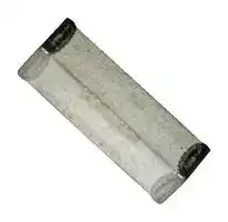
2450AT43B100E
Chip Antenna, 2.45 GHz, 50 Ohm, 7mm x 2mm x 2mm
⚠️ Reference pricing provided. In case of supply shortages, we will connect you with our trusted procurement partners to ensure your project's continuity.
- Manufacturer: JOHANSON TECHNOLOGY
- Product type: Antennas - Single Band Chip
- Centre Frequency:2.45GHz; Antenna Case Size:7mm x 2mm x 2mm; Product Range:-; SVHC:No SVHC (15-Jan-2019)
- SVHC: No SVHC (17-Jan-2023)
- Product Range: -
- Centre Frequency: 2.45GHz
- Antenna Case Size: 7mm x 2mm x 2mm
| Delivery and price | |
|---|---|
| Units per pack | 500 |
| Price | 0.264 € |
| Current stock | 1000+ |
| Lead time | 30 days |
Datasheet

## _**"High Frequency Ceramic Solutions"**_

> **2.4 GHz WLAN, Home RF, Bluetooth Antenna, 802.11 b/g P/N 2450AT43B100 With Ground Clearance Requirements Minimized** Detail Specification: 1/29/2013 Page 1 of 4 **General Specifications Part Number** 2450AT43B100 **Input Power** 2W max. **Frequency Range** 2400 - 2500 Mhz **Impedance** 50 Ω **Peak Gain** 1.3 dBi typ. (XZ-V) **Reel Quanity** 1,000 **Average Gain** -0.5 dBi typ. (XZ-V) **Operating Temperature** -40 to +85°C **Return Loss** 9.5 dB min. **Recommended Storage** +5 to +35°C, Humidity: 45- **Conditions (for unused** 75%RH, 18 mos. Max **product on T&R)**

**Part Number Explanation** Bulk Suffix = S Eg. 2450AT43B100S **Packaging Style** T & R Suffix = E Eg. 2450AT43B100E **P/N Suffix** 100% Tin Suffix = None Eg. 2450AT43B100(E or S) **Termination Style** Tin / Lead Please consult Factory **Evalaution Board** 2450AT43B100-EB1SMA (comes with SMA connector)

**==> picture [447 x 199] intentionally omitted <==**

**----- Start of picture text -----**<br>
Mechanical Dimensions Terminal Configuration<br>pO po<br>In mm No. Function<br>L<br>0.276 ± 0.008 7.00 ± 0.20 1 Feed Point<br>2 ee ee rs ee<br>W 0.079 ± 0.008 2.00 ± 0.20 2 NC<br>a ee ee rsee<br>L1 0.102 ± 0.008 2.60 ± 0.20 3 NC<br>a ee ee rsee<br>W1 0.020 ± 0.008 0.50 ± 0.20 4 NC<br>a ee ee rsee<br>T 0.079 +.004/-.008 2.00 +0.1/-0.2<br>a ee ee<br>a 0.020 ± 0.012 0.50 ± 0.30<br>po<br>L 3<br>a<br>W T 2 1<br>4<br>L1 W1<br>**----- End of picture text -----**<br>


Johanson Technology, Inc. reserves the right to make design changes without notice. All sales are subject to Johanson Technology, Inc. terms and conditions.

**www.johansontechnology.com**

4001 Calle Tecate • Camarillo, CA 93012 • TEL 805.389.1166 FAX 805.389.1821 Ver 1.1 2013 Johanson Technology, Inc.  All Rights Reserved

## _**"High Frequency Ceramic Solutions"**_

> **2.4 GHz WLAN, Home RF, Bluetooth Antenna, 802.11 b/g P/N 2450AT43B100** With Ground Clearance Requirements Minimized Page 2 of 4 Detail Specification: 1/29/2013

## **Mounting and Layout Guidelines:**

Mount these devices with brown mark facing up. Units: mm

**==> picture [419 x 244] intentionally omitted <==**

**----- Start of picture text -----**<br>
*<br>Antenna feed line width should be designed to provide 50  Ω impedance otherwise improper operation will occur<br>Note 1 :  Pins 3 & 4, although "NC", must be soldered to its PCB pads for proper electrical operation<br>With Matching Circuits<br>1  1.6  2.8  1.6  1  1<br>0.8<br>2  2  2.2 nH<br>0.83<br>4.87  0 .8<br>2.7 nH<br>1.83  2<br>10<br>JTI P/N for Matching Circuit:  (Matching circuit and component values will be<br>Inductor (2.2nH): L-07C2N2SV6T  different, depending on PCB layout)<br>Inductor (2.7nH): L-07C2N7SV6T<br>**----- End of picture text -----**<br>


**Note 2:** It is recommended that the designer leave available slots for a "pi" (or shunt-series-shunt) network. The antenna matching network values above are used when antenna is monted on Johanson's evaluation board. The matching values on clinet's PCB will be different. Go to: http://johansontechnology.com/tuning and see how to obtain the new values. If you need further help, contact our RF Applications Eng Team at: http://www.johansontechnology.com/en/ask-a-technical-question.html

**www.johansontechnology.com**

4001 Calle Tecate • Camarillo, CA 93012 • TEL 805.389.1166 FAX 805.389.1821 Ver 1.1 2013 Johanson Technology, Inc.  All Rights Reserved

## _**"High Frequency Ceramic Solutions"**_

**==> picture [446 x 378] intentionally omitted <==**

**----- Start of picture text -----**<br>
2.4 GHz WLAN, Home RF, Bluetooth Antenna, 802.11 b/g P/N 2450AT43B100<br>With Ground Clearance Requirements Minimized Page 3 of 4<br>Detail Specification: 1/29/2013<br>Pe Typical Electrical Characteristics (T=25 [o] C)<br>) ) ) Test Board used orderable p/n: 2450AT43B100-EB1SMA (comes with SMA connector)<br>) ) ) 4.87<br>) Re<br>Antenna<br>co<br>) Ground  10<br>20<br>No Ground<br>Return Loss | $ $ 40   A> |It<br>With Matching Circuit<br>ia)<br>-§<br>= -10 ) P<br>**----- End of picture text -----**<br>


Johanson Technology, Inc. reserves the right to make design changes without notice. All sales are subject to Johanson Technology, Inc. terms and conditions.

**www.johansontechnology.com**

4001 Calle Tecate • Camarillo, CA 93012 • TEL 805.389.1166 FAX 805.389.1821 Ver 1.1 2013 Johanson Technology, Inc.  All Rights Reserved

## _**"High Frequency Ceramic Solutions"**_

**==> picture [446 x 497] intentionally omitted <==**

**----- Start of picture text -----**<br>
2.4 GHz WLAN, Home RF, Bluetooth Antenna, 802.11 b/g P/N 2450AT43B100<br>With Ground Clearance Requirements Minimized Page 4 of 4<br>Detail Specification: 1/29/2013<br>Pe Typical Electrical Characteristics/Radiation Patterns (T=25 [o] C)<br>) ) ) XY cut @2.45GHz  318. Ase<br>XY-V/XY-H Z  )     Vertical     Horizontal  300/ (fo NS “TV\\ eo PSbeg / = 60<br>) ) )<br>180°<br>)<br>90°  a - —_ =——= —_ X  \tT (do 3020" \_Y-10" + lage<br>—— yo ~y ai AV SEI<br>‘ , 270°  Ko SOY<br>Y  0°  2400. IQ. \ 7 SS JU 420<br>XY-cut scanning direction  228 \ f TSA “136<br>:<br>woe 30<br>XZ-V/XZ-H Y  XZ cut @2.45GHz     Vertical  318, AX \ / a 45<br>    Horizontal<br>180°<br>= 285, /X</™ LY \ 75<br>X<br>90°<br>270°<br>~ 7 7 a \ \SSSTwa HE.i<br>Z  0°<br>XZ-cut scanning direction  NO228 OK ; TDs J, \<br>210JT sO aa<br>YZ cut @2.45GHz )     Vertical<br>    Horizontal<br>YZ-V/YZ-H X<br>) 00 Vien .XS ON <\ do<br>180°<br>=-_- _ = 205//)/aaNy_ ~\Seyi\\ Vs<br>Y<br>~~-JjW_--_- HIRST AY<br>90°  li Pp Fia one eee<br>x 7 a 270°  AV SAT LJ<br>— _ - =“ \ \\ AY J ros<br>Z  Weer 0°   Se 240\\ dSSe Z Shaf / 120<br>YZ-cut scanning direction<br>**----- End of picture text -----**<br>


Johanson Technology, Inc. reserves the right to make design changes without notice. All sales are subject to Johanson Technology, Inc. terms and conditions.

**www.johansontechnology.com**

4001 Calle Tecate • Camarillo, CA 93012 • TEL 805.389.1166 FAX 805.389.1821 Ver 1.1 2013 Johanson Technology, Inc.  All Rights Reserved
Updated at April 22, 2026
About Novapart
Novapart is a B2B electronic component broker specialising in stock shortages and cost reduction. We source hard-to-find parts and identify compliant alternatives across a catalogue of 410,000+ components from 500+ manufacturers.
Learn more →Stock Shortage Specialist
When a component is unavailable, discontinued or has an unacceptable lead time, we tap into our network of vetted European and Asian distributors to source what you need — without compromising on quality or traceability.
Request a quote →Compliant Alternatives
We identify pin-to-pin, electrically equivalent substitutes that meet the same certifications (RoHS, AEC-Q100, REACH) as your original specification — validated against datasheets, not just part numbers. Often at a lower cost.
BOM Analysis service →