


1SMA24AT3G
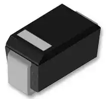
TVS Diode, SMA Series, Unidirectional, 24 V, 38.9 V, DO-214AC (SMA), 2 Pins
- Manufacturer: ONSEMI
- Product type: TVS Diodes
- Available until stocks are exhausted
- SVHC: No SVHC (15-Jan-2018)
- No. of Pins: 2Pins
- TVS Polarity: Unidirectional
- Product Range: SMA Series
- Qualification: -
- Diode Mounting: Surface Mount
- Diode Case Style: DO-214AC (SMA)
- Clamping Voltage Max: 38.9V
- Reverse Standoff Voltage: 24V
- Maximum Breakdown Voltage: 29.5V
- Minimum Breakdown Voltage: 26.7V
- Operating Temperature Max: 150°C
- Peak Pulse Power Dissipation: 400W
| Delivery and price | |
|---|---|
| Units per pack | 1000 |
| Price | 0.151 € |
| Current stock | 1000+ |
| Lead time | 30 days |
Surface Mount  >  400W  >  1SMA5.0AT3G Series

~~Pb @~~

## **TVS Diodes**

## 1SMA5.0AT3G Series

## **Description**

The 1SMA5.0AT3G series is designed to protect voltage sensitive components from high voltage, high energy transients. They have excellent clamping capability, high surge capability, low zener impedance and fast response time. The 1SMA5.0AT3G series is supplied in the Littelfuse exclusive, cost-effective, highly reliable package and is ideally suited for use in communication systems, automotive, numerical controls, process controls, medical equipment, business machines, power supplies and many other industrial/consumer applications.

**Maximum Ratings and Thermal Characteristics** Po Parameter Symbol Value Unit Peak Power Dissipation (Note 1) @ T25°C, Pulse Width = 1 ms L = PPK 400 W DC Power Dissipation @ TMeasured Zero Lead Length (Note 2) L = 75°C PD 1.0 W Derate Above 75°C 20 mW/°C Thermal Resistance from Junction to−Lead R JL 50 °C/W DC Power Dissipation (Note 3) @ TA = 25°C PD 0.5 W Derate Above 25°C 4.0 mW/°C Thermal Resistance from Junction–to– R0JA 250 °C/W Ambient Forward Surge Current (Note 4) @ TA = 25°C IFSM 40 A Operating and Storage Temperature -65 to T T °C Range J, stg +150 ~~=m~~ Stresses exceeding those listed in the Maximum Ratings table may damage the device. If any of these limits are exceeded, device functionality should not be assumed, damage may occur and reliability may be affected.

## **Features** Po • Working Peak Reverse Voltage Range − 5.0 V to 78 V • Standard Zener Breakdown Voltage Range − 6.7 V to 91.25 V • Peak Power − 400 W @ 1 ms • ESD Rating of Class 3 (> 16 kV) per Human Body Model • Response Time is Typically < 1 ns • Flat Handling Surface for Accurate Placement • Package Design for Top Slide or Bottom Circuit Board Moun ~~ting~~ • Low Profile Package • These are Pb−Free Device **Functional Diagram** Cathode Anode Additional Information ~~Lo~~ Gi **Datasheet Resources Samples**

1. 10 X 1000 µs, non−repetitive.

2. 1” square copper pad, FR−4 board.

3. FR−4 board, using Littelfuse minimum recommended footprint, as shown in 403D-02 case outline dimensions spec.

4. 1/2 sine wave (or equivalent square wave), PW = 8.3 ms, duty cycle = 4 pulses per minute maximum.

© 2017 Littelfuse, Inc. Specifications are subject to change without notice. Revised: 09/14/17

**TVS Diodes**

Surface Mount  >  400W  >  1SMA5.0AT3G Series

**==> picture [94 x 32] intentionally omitted <==**

**==> picture [504 x 198] intentionally omitted <==**

**----- Start of picture text -----**<br>
I-V Curve Characteristics (TA = 25°C unless otherwise noted, VF = 3.5 V Max. @ IF = 30 A for all types) (Note 5)<br>I Symbol Parameter<br>IF IPP Maximum Reverse Peak Pulse Current<br>VC Clamping Voltage @ IPP<br>VRWM Working Peak Reverse Voltage<br>VC VBR VRWM V IR Maximum Reverse Leakage Current @ VRWM<br>IR VF<br>IT VBR Breakdown Voltage @ IT<br>IT Test Current<br>IPP IF Maximum Temperature Coefficient of VBR<br>VF Forward Voltage @ IF<br>**----- End of picture text -----**<br>


5. 1/2 sine wave or equivalent, PW = 8.3 ms, non−repetitive duty cycle.

5. 1/2 sine wave or equivalent, PW = 8.3 ms non−repetitive duty cycle

© 2017 Littelfuse, Inc. Specifications are subject to change without notice. Revised: 09/14/17

**TVS Diodes**

Surface Mount  >  400W  >  1SMA5.0AT3G Series

**==> picture [94 x 32] intentionally omitted <==**

## **Electrical Characteristics**

**==> picture [505 x 547] intentionally omitted <==**

**----- Start of picture text -----**<br>
Breakdown Voltage VC @ IPP<br>(Note 8)<br>V I  @  C Typ.<br>Device*  Device  (Note 6)RWM VRRWM VBR @ IT (V) (Note 7) @ IT VC IPP (Note 9)<br>Marking<br>Volts µA MIN NOM MAX mA Volts  Amps pF<br>1SMA5.0AT3G QE 5.0 400 6.4 6.7 7.0 10 9.2 43.5 2035<br>1SMA6.0AT3G QG 6.0 400 6.67 7.02 7.37 10 10.3 38.8 1730<br>1SMA6.5AT3G QK 6.5 250 7.22 7.6 7.98 10 11.2 35.7 1605<br>1SMA8.0AT3G QR 8.0 25 8.89 9.36 9.83 1 13.6 29.4 1035<br>1SMA8.5AT3G QT 8.5 5.0 9.44 9.92 10.4 1 14.4 27.8 1265<br>1SMA9.0AT3G QV 9.0 2.5 10 10.55 11.1 1 15.4 26.0 1200<br>1SMA10AT3G QX 10 2.5 11.1 11.7 12.3 1 17.0 23.5 1090<br>1SMA11AT3G QZ 11 2.5 12.2 12.85 13.5 1 18.2 22.0 1000<br>1SMA12AT3G RE 12 2.5 13.3 14.0 14.7 1 19.9 20.1 925<br>1SMA13AT3G RG 13 2.5 14.4 15.15 15.9 1 21.5 18.6 860<br>1SMA14AT3G RH 14 2.5 15.6 16.4 17.2 1 23.2 17.2 800<br>1SMA15AT3G RM 15 2.5 16.7 17.6 18.5 1 24.4 16.4 758<br>1SMA16AT3G RP 16 2.5 17.8 18.75 19.7 1 26.0 15.4 715<br>1SMA17AT3G RR 17 2.5 18.9 19.9 20.9 1 27.6 14.5 680<br>1SMA18AT3G RT 18 2.5 20 21.05 22.1 1 29.2 13.7 645<br>1SMA20AT3G RV 20 2.5 22.2 23.35 24.5 1 32.4 12.3 585<br>1SMA22AT3G RX 22 2.5 24.4 25.65 26.9 1 35.5 11.3 540<br>1SMA24AT3G RZ 24 2.5 26.7 28.1 29.5 1 38.9 10.3 500<br>1SMA26AT3G SE 26 2.5 28.9 30.4 31.9 1 42.1 9.5 460<br>1SMA28AT3G SG 28 2.5 31.1 32.75 34.4 1 45.4 8.8 430<br>1SMA30AT3G SK 30 2.5 33.3 35.05 36.8 1 48.4 8.3 405<br>1SMA33AT3G SM 33 2.5 36.7 38.65 40.6 1 53.3 7.5 375<br>1SMA36AT3G SP 36 2.5 40 42.1 44.2 1 58.1 6.9 345<br>1SMA40AT3G SR 40 2.5 44.4 46.75 49.1 1 64.5 6.2 315<br>1SMA43AT3G ST 43 2.5 47.8 50.3 52.8 1 69.4 5.8 295<br>1SMA45AT3G SV 45 2.5 50 52.65 55.3 1 72.2 5.5 280<br>1SMA48AT3G SX 48 2.5 53.3 56.1 58.9 1 77.4 5.2 265<br>1SMA54AT3G TE 54 2.5 60 63.15 66.3 1 87.1 4.6 240<br>1SMA58AT3G TG 58 2.5 64.4 67.8 71.5 1 93.6 4.3 225<br>1SMA70AT3G TP 70 2.5 77.8 81.9 86.0 1 113 3.5 190<br>**----- End of picture text -----**<br>


6. A transient suppressor is normally selected according to the working peak reverse voltage (VRWM), which should be equal to or greater than the DC or continuous peak operating voltage level.

7. VBR measured at pulse test current IT at an ambient temperature of 25°C.

8. Surge current waveform per Figure 2 and derate per Figure 3.

9. Bias voltage = 0 V, F = 1.0 MHz, TJ = 25°C.

- †Please see 1SMA10CAT3 to 1SMA75CAT3 for Bidirectional devices.

© 2017 Littelfuse, Inc. Specifications are subject to change without notice. Revised: 09/14/17

**TVS Diodes**

Surface Mount  >  400W  >  1SMA5.0AT3G Series

**==> picture [94 x 32] intentionally omitted <==**

## **Ratings and Characteristic Curves**

**==> picture [244 x 194] intentionally omitted <==**

**----- Start of picture text -----**<br>
Figure 1. Pulse Rating Curve<br>100<br>NONREPETITIVE<br>PULSE WAVEFORM<br>SHOWN IN FIGURE 2.<br>10 TA = 25°C<br>1<br>0.1<br>10 4 0.001 0.01 0.11 10<br>tP, PULSE WIDTH (ms)<br>, PEAK POWER (kW)<br>pk<br>P<br>**----- End of picture text -----**<br>


**Figure 3 - Pulse Derating Curve**

**==> picture [244 x 171] intentionally omitted <==**

**==> picture [244 x 19] intentionally omitted <==**

**----- Start of picture text -----**<br>
Figure 2. Pulse Waveform<br>**----- End of picture text -----**<br>


**==> picture [243 x 171] intentionally omitted <==**

## **Figure 4. Typical Junction Capacitance vs. Bias Voltage**

**==> picture [244 x 171] intentionally omitted <==**

**----- Start of picture text -----**<br>
10,000<br>TJ = 25°C<br>F = 1 MHz<br>1SMA5.0AT3G<br>1,000<br>1SMA10AT3G<br>1SMA36AT3G<br>100<br>1SMA64AT3G<br>10<br>1<br>1 10 100<br>BIAS VOLTAGE (VOLTS)<br>C, CAPACITANCE (pF)<br>**----- End of picture text -----**<br>


**==> picture [243 x 195] intentionally omitted <==**

**----- Start of picture text -----**<br>
Figure 5. Steady State Power Derating<br>6<br>5<br>4<br>3 @ TL = 75°C<br>PD = 1.5 W<br>2<br>@ TA = 25°C<br>1 PD = 0.5 W<br>0<br>0 25 50 75 100 125 150<br>T, TEMPERATURE (°C)<br>PD, MAXIMUM POWER DISSIPATION (WATTS)<br>**----- End of picture text -----**<br>


© 2017 Littelfuse, Inc. Specifications are subject to change without notice. Revised: 09/14/17

**TVS Diodes**

Surface Mount  >  400W  >  1SMA5.0AT3G Series

**==> picture [94 x 32] intentionally omitted <==**

**==> picture [245 x 19] intentionally omitted <==**

**----- Start of picture text -----**<br>
Dimensions<br>**----- End of picture text -----**<br>


**==> picture [172 x 129] intentionally omitted <==**

**----- Start of picture text -----**<br>
HE<br>E<br>bD D<br>POLARITY INDICATOR<br>OPTIONAL AS NEEDED<br>(SEE STYLES)<br>A<br>A1<br>L c<br>**----- End of picture text -----**<br>


**==> picture [245 x 161] intentionally omitted <==**

**----- Start of picture text -----**<br>
Inches Millimeters<br>Dim<br>Min Nom Max Min Nom Max<br>A 0.078 0.083 0.087 1.97 2.10 2.20<br>A1 0.002 0.004 0.008 0.05 0.10 0.20<br>b 0.050 0.057 0.064 1.27 1.45 1.63<br>c 0.006 0.011 0.016 0.15 0.28 0.41<br>D 0.090 0.103 0.115 2.29 2.60 2.92<br>E 0.160 0.170 0.180 4.06 4.32 4.57<br>HE 0.190 0.205 0.220 4.83 5.21 5.59<br>L 0.030 0.045 0.060 0.76 1.14 1.52<br>**----- End of picture text -----**<br>


NOTES:

1. DIMENSIONING AND TOLERANCING PER ANSI Y14.5M, 1982.

2. CONTROLLING DIMENSION: INCH.

3. DIMENSION b SHALL BE MEASURED WITHIN DIMENSION L.

## STYLE 1:

PIN 1. CATHODE (POLARITY BAND)

2. ANODE

## **Part Marking System**

**==> picture [47 x 38] intentionally omitted <==**

**----- Start of picture text -----**<br>
xx<br>WW<br>AY<br>**----- End of picture text -----**<br>


xx = Device Code (Refer to page 3) A= Assembly Location Y= Year WW = Work Week

## **Soldering Footrpint**

**==> picture [247 x 497] intentionally omitted <==**

**----- Start of picture text -----**<br>
4.000<br>0.157<br>2.000<br>0.079<br>2.000<br>0.079<br>SCALE 8:1 mm<br>inches<br>ORDERING INFORMATION<br>Device Package Shipping†<br>SMA 5,000 /<br>1SMAxxAT3G<br>(Pb−Free) Tape & Reel<br>Flow/Wave Soldering (Solder Dipping)<br>Peak Temperature : 260 [O] C<br>Dipping Time : 10 seconds<br>Physical Specifications<br>Void-free, transfer-molded, thermosetting<br>Case<br>plastic<br>Cathode indicated by molded polarity<br>Polarity<br>notch<br>Mounting Position Any<br>All external surfaces are corrosion<br>Finish<br>resistant and leads are readily solderable<br>**----- End of picture text -----**<br>


**Disclaimer Notice** - Information furnished is believed to be accurate and reliable. However, users should independently evaluate the suitability of and test each product selected for their own applications. Littelfuse products are not designed for, and may not be used in, all applications. Read complete Disclaimer Notice at: www.littelfuse.com/disclaimer-electronics.

© 2017 Littelfuse, Inc. Specifications are subject to change without notice. Revised: 09/14/17
Updated at June 1, 2026
onsemi is a premier global supplier of intelligent power and sensing technologies, driving disruptive innovations across the automotive, industrial, and cloud infrastructure markets. Recognized for their commitment to sustainability and reliable supply chains, the company accelerates advancements in vehicle electrification, industrial automation, and 5G networks by solving the industry's most complex design challenges. At the core of their portfolio is an industry-leading selection of discrete semiconductors. This extensive range features thousands of high-performance bipolar transistors, single and dual MOSFETs, and a comprehensive array of diodes, including Zener, Schottky, and fast-recovery rectifiers. Engineered for superior thermal performance and energy efficiency, these foundational components are critical for demanding power conversion, switching, and signal conditioning applications. Beyond essential discretes, onsemi provides a robust suite of advanced power management and circuit protection solutions. Their lineup includes intelligent power modules, single IGBTs, and transient voltage suppression (TVS) diodes designed to safeguard sensitive circuitry. Complimented by integrated passive filters, AC/DC LED driver ICs, and specialized sub-2.4GHz RF transceivers, onsemi equips engineers with the scalable, high-quality technologies needed to build a cleaner, smarter, and more connected world.
About Novapart
Novapart is a B2B electronic component broker specialising in stock shortages and cost reduction. We source hard-to-find parts and identify compliant alternatives across a catalogue of 410,000+ components from 500+ manufacturers.
Learn more →Stock Shortage Specialist
When a component is unavailable, discontinued or has an unacceptable lead time, we tap into our network of vetted European and Asian distributors to source what you need — without compromising on quality or traceability.
Request a quote →Compliant Alternatives
We identify pin-to-pin, electrically equivalent substitutes that meet the same certifications (RoHS, AEC-Q100, REACH) as your original specification — validated against datasheets, not just part numbers. Often at a lower cost.
BOM Analysis service →