


1N5927BG
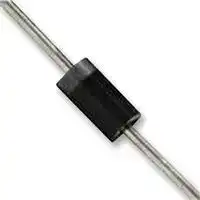
Zener Single Diode, Surmetic, 12 V, 3 W, DO-41 (DO-204AL), 5 %, 2 Pins, 200 °C
- Manufacturer: ONSEMI
- Product type: Zener Single Diodes
- Zener Voltage Vz Typ:12V; Power Dissipation Pd:3W; Diode Case Style:Axial Leaded; Zener Tolerance ±:5%; No. of Pins:2Pins; Operating Temperature Max:200°C; Product Range:1N5927 Series; Automotive
- SVHC: Lead (25-Jun-2025)
- No. of Pins: 2Pins
- Product Range: 1N5927
- Qualification: -
- Diode Mounting: Through Hole
- Diode Case Style: DO-41 (DO-204AL)
- Power Dissipation: 3W
- Zener Voltage Nom: 12V
- Operating Temperature Max: 200°C
| Delivery and price | |
|---|---|
| Units per pack | 5000 |
| Price | 0.117 € |
| Current stock | 200+ |
| Lead time | 30 days |
## 1N5913B Series

## 1N5913B Series 3 W DO−41 Surmetic 30 Zener Voltage Regulators This is a complete series of 3 W Zener diodes with limits and —

## Zener Voltage Regulators

This is a complete series of 3 W Zener diodes with limits and excellent operating characteristics that reflect the superior capabilities of silicon−oxide passivated junctions. All this in an axial−lead, transfer−molded plastic package that offers protection in all common environmental conditions.

## **http://onsemi.com**

## **Features**

Cathode Anode • Zener Voltage Range − 3.3 V to 200 V • ESD Rating of Class 3 (>16 KV) per Human Body Model • Surge Rating of 98 W @ 1 ms • Maximum Limits Guaranteed on up to Six Electrical Parameters • Package No Larger than the Conventional 1 W Package **AXIAL LEAD CASE 59** • Pb−Free Packages are Available **PLASTIC STYLE 1 Mechanical Characteristics CASE:** Void free, transfer−molded, thermosetting plastic **MARKING DIAGRAM FINISH:** All external surfaces are corrosion resistant and leads are readily solderable A **MAXIMUM LEAD TEMPERATURE FOR SOLDERING PURPOSES:** 1N 260°C, 1/16″ from the case for 10 seconds YYWW59xxB **POLARITY:** Cathode indicated by polarity band {C ~~5~~ **MOUNTING POSITION:** Any A = Assembly Location 1N59xxB = Device Number **MAXIMUM RATINGS** YY = Year WW = Work Week **Rating Symbol Value Unit** = Pb−Free Package Max. Steady State Power Dissipation PD 3 W (Note: Microdot may be in either location) @ TL = 75 ° C, Lead Length = 3/8 ″ Derate above 75 ° C 24 mW/ ° C **ORDERING INFORMATION** Steady State Power Dissipation PD 1 W @ TA = 50 ° C **Device Package Shipping**[†] Derate above 50 ° C 6.67 mW/ ° C 1N59xxB, G Axial Lead 2000 Units/Box Operating and Storage TJ, Tstg −65 to ° C (Pb−Free) Temperature Range +200 1N59xxBRL, G Axial Lead 6000/Tape & Reel Maximum ratings are those values beyond which device damage can occur. (Pb−Free) ~~HE =~~ Maximum ratings applied to the device are individual stress limit values (not normal operating conditions) and are not valid simultaneously. If these limits are †For information on tape and reel specifications, exceeded, device functional operation is not implied, damage may occur and including part orientation and tape sizes, please reliability may be affected. refer to our Tape and Reel Packaging Specification Brochure, BRD8011/D.

*For additional information on our Pb−Free strategy  and soldering details, please download the ON Semiconductor Soldering and Mounting Techniques Reference Manual, SOLDERRM/D.

Publication Order Number:

**1**

© Semiconductor Components Industries, LLC, 2006 **April, 2006 − Rev. 5**

**1N5913B/D**

**1N5913B Series**

## **ELECTRICAL CHARACTERISTICS**

(TL = 30 ° C unless otherwise noted,

VF = 1.5 V Max @ IF = 200 mAdc for all types)

|**Symbol**|**Parameter**|
|---|---|
|VZ|Reverse Zener Voltage @ IZT|
|IZT|Reverse Current|
|ZZT|Maximum Zener Impedance @ IZT|
|IZK|Reverse Current|
|ZZK|Maximum Zener Impedance @ IZK|
|IR|Reverse Leakage Current @ VR|
|VR|Breakdown Voltage|
|IF|Forward Current|
|VF|Forward Voltage @ IF|
|IZM|Maximum DC Zener Current|


**==> picture [181 x 177] intentionally omitted <==**

**----- Start of picture text -----**<br>
I<br>IF<br>VZ VR V<br>IR VF<br>IZT<br>Zener Voltage Regulator<br>**----- End of picture text -----**<br>


**http://onsemi.com**

**2**

## **1N5913B Series**

**ELECTRICAL CHARACTERISTICS** (TL = 30 ° C unless otherwise noted, VF = 1.5 V Max @ IF = 200 mAdc for all types)

|**Device**†<br>(Note 1)|**Device**<br>**Marking**|**Zener Voltage**(Note 2)|**Zener Voltage**(Note 2)|**Zener Voltage**(Note 2)|**Zener Voltage**(Note 2)|**Zener Impedance**(Note 3)|**Zener Impedance**(Note 3)|**Zener Impedance**(Note 3)|**Leakage Current**|**Leakage Current**|**IZM**|
|---|---|---|---|---|---|---|---|---|---|---|---|
||||**VZ (Volts)**||**@ IZT**|**ZZT @ IZT**|**ZZK @ IZK**||**IR @ VR**|||
|||**Min**|**Nom**|**Max**|**mA**|�|�|**mA**|�**A Max**|**Volts**|**mA**|
|1N5913B, G<br>1N5917B, G<br>1N5919B, G<br>**_1N5920B, G_**<br>1N5921B, G|1N5913B<br>1N5917B<br>1N5919B<br>**_1N5920B_**<br>1N5921B|3.14<br>4.47<br>5.32<br>**_5.89_**<br>6.46|3.3<br>4.7<br>5.6<br>**_6.2_**<br>6.8|3.47<br>4.94<br>5.88<br>**_6.51_**<br>7.14|113.6<br>79.8<br>66.9<br>**_60.5_**<br>55.1|10<br>5<br>2<br>**_2_**<br>2.5|500<br>500<br>250<br>**_200_**<br>200|1<br>1<br>1<br>**_1_**<br>1|100<br>5<br>5<br>**_5_**<br>5|1<br>1.5<br>3<br>**_4_**<br>5.2|454<br>319<br>267<br>**_241_**<br>220|
|1N5923B, G<br>1N5924B, G<br>1N5925B, G<br>1N5926B, G<br>1N5927B, G|1N5923B<br>1N5924B<br>1N5925B<br>1N5926B<br>1N5927B|7.79<br>8.65<br>9.50<br>10.45<br>11.40|8.2<br>9.1<br>10<br>11<br>12|8.61<br>9.56<br>10.50<br>11.55<br>12.60|45.7<br>41.2<br>37.5<br>34.1<br>31.2|3.5<br>4<br>4.5<br>5.5<br>6.5|400<br>500<br>500<br>550<br>550|0.5<br>0.5<br>0.25<br>0.25<br>0.25|5<br>5<br>5<br>1<br>1|6.5<br>7<br>8<br>8.4<br>9.1|182<br>164<br>150<br>136<br>125|
|**_1N5929B, G_**<br>1N5930B, G<br>1N5931B, G<br>1N5932B, G<br>1N5933B, G|**_1N5929B_**<br>1N5930B<br>1N5931B<br>1N5932B<br>1N5933B|**_14.25_**<br>15.20<br>17.10<br>19.00<br>20.90|**_15_**<br>16<br>18<br>20<br>22|**_15.75_**<br>16.80<br>18.90<br>21.00<br>23.10|**_25.0_**<br>23.4<br>20.8<br>18.7<br>17.0|**_9_**<br>10<br>12<br>14<br>17.5|**_600_**<br>600<br>650<br>650<br>650|**_0.25_**<br>0.25<br>0.25<br>0.25<br>0.25|**_1_**<br>1<br>1<br>1<br>1|**_11.4_**<br>12.2<br>13.7<br>15.2<br>16.7|**_100_**<br>93<br>83<br>75<br>68|
|1N5934B, G<br>1N5935B, G<br>**_1N5936B, G_**<br>1N5937B, G<br>1N5938B, G|1N5934B<br>1N5935B<br>**_1N5936B_**<br>1N5937B<br>1N5938B|22.80<br>25.65<br>**_28.50_**<br>31.35<br>34.20|24<br>27<br>**_30_**<br>33<br>36|25.20<br>28.35<br>**_31.50_**<br>34.65<br>37.80|15.6<br>13.9<br>**_12.5_**<br>11.4<br>10.4|19<br>23<br>**_28_**<br>33<br>38|700<br>700<br>**_750_**<br>800<br>850|0.25<br>0.25<br>**_0.25_**<br>0.25<br>0.25|1<br>1<br>**_1_**<br>1<br>1|18.2<br>20.6<br>**_22.8_**<br>25.1<br>27.4|62<br>55<br>**_50_**<br>45<br>41|
|1N5940B, G<br>1N5941B, G<br>1N5942B, G<br>1N5943B, G<br>1N5944B, G|1N5940B<br>1N5941B<br>1N5942B<br>1N5943B<br>1N5944B|40.85<br>44.65<br>48.45<br>53.20<br>58.90|43<br>47<br>51<br>56<br>62|45.15<br>49.35<br>53.55<br>58.80<br>65.10|8.7<br>8.0<br>7.3<br>6.7<br>6.0|53<br>67<br>70<br>86<br>100|950<br>1000<br>1100<br>1300<br>1500|0.25<br>0.25<br>0.25<br>0.25<br>0.25|1<br>1<br>1<br>1<br>1|32.7<br>35.8<br>38.8<br>42.6<br>47.1|34<br>31<br>29<br>26<br>24|
|1N5946B, G<br>1N5947B, G<br>1N5948B, G<br>1N5950B, G|1N5946B<br>1N5947B<br>1N5948B<br>1N5950B|71.25<br>77.90<br>86.45<br>104.5|75<br>82<br>91<br>110|78.75<br>86.10<br>95.55<br>115.5|5.0<br>4.6<br>4.1<br>3.4|140<br>160<br>200<br>300|2000<br>2500<br>3000<br>4000|0.25<br>0.25<br>0.25<br>0.25|1<br>1<br>1<br>1|56<br>62.2<br>69.2<br>83.6|20<br>18<br>16<br>13|
|1N5951B, G<br>1N5952B, G<br>1N5953B, G<br>1N5954B, G<br>**_1N5955B, G_**|1N5951B<br>1N5952B<br>1N5953B<br>1N5954B<br>**_1N5955B_**|114<br>123.5<br>142.5<br>152<br>**_171_**|120<br>130<br>150<br>160<br>**_180_**|126<br>136.5<br>157.5<br>168<br>**_189_**|3.1<br>2.9<br>2.5<br>2.3<br>**_2.1_**|380<br>450<br>600<br>700<br>**_900_**|4500<br>5000<br>6000<br>6500<br>**_7000_**|0.25<br>0.25<br>0.25<br>0.25<br>**_0.25_**|1<br>1<br>1<br>1<br>**_1_**|91.2<br>98.8<br>114<br>121.6<br>**_136.8_**|12<br>11<br>10<br>9<br>**_8_**|
|1N5956B, G|1N5956B|190|200|210|1.9|1200|8000|0.25|1|152|7|


Devices listed in _**bold, italic**_ are ON Semiconductor **Preferred** devices. **Preferred** devices are recommended choices for future use and best overall value.

†The “G’’ suffix indicates Pb−Free package available.

1. **TOLERANCE AND TYPE NUMBER DESIGNATION**

Tolerance designation − device tolerance of ± 5% are indicated by a “B” suffix.

## 2. **ZENER VOLTAGE (VZ) MEASUREMENT**

ON Semiconductor guarantees the zener voltage when measured at 90 seconds while maintaining the lead temperature (TL) at 30 ° C ± 1 ° C, 3/8 ″ from the diode body.

3. **ZENER IMPEDANCE (ZZ) DERIVATION**

The zener impedance is derived from 60 seconds AC voltage, which results when an AC current having an rms value equal to 10% of the DC zener current (IZT or IZK) is superimposed on IZT or IZK.

**http://onsemi.com**

**3**

**1N5913B Series**

**==> picture [241 x 168] intentionally omitted <==**

**----- Start of picture text -----**<br>
5<br>L = LEAD LENGTH<br>L = 1/8″       TO HEAT SINK<br>4<br>L = 3/8″<br>3<br>2 L = 1″<br>1<br>0<br>0 20 40 60 80 100 120 140 160 180 200<br>TL, LEAD TEMPERATURE ( ° C)<br>, STEADY STATE DISSIPATION (WATTS)<br>D<br>P<br>**----- End of picture text -----**<br>


**Figure 1. Power Temperature Derating Curve**

**==> picture [491 x 165] intentionally omitted <==**

**----- Start of picture text -----**<br>
30<br>20<br>D =0.5<br>10<br>7 0.2<br>5<br>0.1<br>3<br>0.05 PPK t1<br>2 t2<br>0.02 DUTY CYCLE, D =t1/t2<br>1<br>0.7 0.01 NOTE: BELOW 0.1 SECOND, THERMAL  SINGLE PULSE �TJL = �JL (t)PPK<br>0.5 D = 0                 RESPONSE CURVE IS APPLICABLE  REPETITIVE PULSES �TJL = �JL (t,D)PPK<br> TO ANY LEAD LENGTH (L).<br>0.3<br>0.0001 0.0002 0.0005 0.001 0.002 0.005 0.01 0.02 0.05 0.1 0.2 0.5 1 2 5 10<br>t, TIME (SECONDS)<br>°<br>   JUNCTION-TO-LEAD (  C/W)<br>JL(t, D) TRANSIENT THERMAL RESISTANCE<br>θ<br>**----- End of picture text -----**<br>


**Figure 2. Typical Thermal Response L, Lead Length = 3/8 Inch**

**==> picture [491 x 162] intentionally omitted <==**

**----- Start of picture text -----**<br>
1K<br>2 [3]<br>RECTANGULAR<br>500 NONREPETITIVEWAVEFORM 0.51 TA = 125°C<br>300 TJ�=�25°C PRIOR 0.2<br>200 TO INITIAL PULSE 0.1<br>0.05<br>100<br>0.02<br>0.01<br>50<br>0.005<br>30 0.002 TA = 125°C<br>20 0.001<br>0.0005<br>0.0003<br>10 1 2 5 10 20 50 100 200 400 1000<br>0.1 0.2 0.3 0.5 1 2 3 5 10 20 30 50 100<br>PW, PULSE WIDTH (ms) NOMINAL VZ (VOLTS)<br>Adc) @ VR<br>μ<br>P     , PEAK SURGE POWER (WATTS)PK IR, REVERSE LEAKAGE ( AS SPECIFIED IN ELEC. CHAR. TABLE<br>**----- End of picture text -----**<br>


**Figure 3. Maximum Surge Power**

**Figure 4. Typical Reverse Leakage**

**http://onsemi.com**

**4**

**1N5913B Series**

## **APPLICATION NOTE**

Since the actual voltage available from a given zener diode is temperature dependent, it is necessary to determine junction temperature under any set of operating conditions in order to calculate its value. The following procedure is recommended:

Lead Temperature, TL, should be determined from:

TL = � LA PD + TA

�LA is the lead-to-ambient thermal resistance (°C/W) and PD is the power dissipation. The value for �LA will vary and depends on the device mounting method. �LA is generally 30−40°C/W for the various clips and tie points in common use and for printed circuit board wiring.

The temperature of the lead can also be measured using a thermocouple placed on the lead as close as possible to the tie point. The thermal mass connected to the tie point is normally large enough so that it will not significantly respond to heat surges generated in the diode as a result of pulsed operation once steady-state conditions are achieved. Using the measured value of TL, the junction temperature may be determined by:

**==> picture [60 x 10] intentionally omitted <==**

�TJL is the increase in junction temperature above the lead temperature and may be found from Figure 2 for a train of power pulses (L = 3/8 inch) or from Figure 10 for dc power.

� TJL = � JL PD

For worst-case design, using expected limits of IZ, limits of PD and the extremes of TJ (�TJ) may be estimated. Changes in voltage, VZ, can then be found from:

**==> picture [56 x 10] intentionally omitted <==**

�VZ, the zener voltage temperature coefficient, is found from Figures 5 and 6.

Under high power-pulse operation, the zener voltage will vary with time and may also be affected significantly by the zener resistance. For best regulation, keep current excursions as low as possible.

Data of Figure 2 should not be used to compute surge capability. Surge limitations are given in Figure 3. They are lower than would be expected by considering only junction temperature, as current crowding effects cause temperatures to be extremely high in small spots resulting in device degradation should the limits of Figure 3 be exceeded.

**http://onsemi.com**

**5**

**1N5913B Series**

## **TEMPERATURE COEFFICIENT RANGES**

(90% of the Units are in the Ranges Indicated)

**==> picture [490 x 177] intentionally omitted <==**

**----- Start of picture text -----**<br>
10 1000<br>8 500<br>6<br>200<br>4<br>100<br>2 RANGE<br>50<br>0<br>−2 20<br>−4 10<br>3 4 5 6 7 8 9 10 11 12 10 20 50 100 200 400 1000<br>VZ, ZENER VOLTAGE @ IZT (VOLTS) VZ, ZENER VOLTAGE @ IZT (VOLTS)<br>°<br>°<br>, TEMPERATURE COEFFICIENT (mV/  C) @ IZT<br>, TEMPERATURE COEFFICIENT (mV/  C) @ IZT<br>VZ<br>θ VZ<br>θ<br>**----- End of picture text -----**<br>


**Figure 5. Units To 12 Volts**

**Figure 6. Units 10 To 400 Volts**

## **ZENER VOLTAGE versus ZENER CURRENT**

(Figures 7, 8 and 9)

**==> picture [491 x 374] intentionally omitted <==**

**----- Start of picture text -----**<br>
100 100<br>50 50<br>30 30<br>20 20<br>10 10<br>5 5<br>3 3<br>2 2<br>1 1<br>0.5 0.5<br>0.3 0.3<br>0.2 0.2<br>0.1 0.1<br>0 1 2 3 4 5 6 7 8 9 10 0 10 20 30 40 50 60 70 80 90 100<br>VZ, ZENER VOLTAGE (VOLTS) VZ, ZENER VOLTAGE (VOLTS)<br>Figure 7. VZ = 3.3 thru 10 Volts Figure 8. VZ = 12 thru 82 Volts<br>10 80<br>70<br>5<br>60<br>2 50<br>1 40 L L<br>30<br>0.5 T L<br>20<br>PRIMARY PATH OF<br>0.2 10 CONDUCTION IS THROUGH<br>THE CATHODE LEAD<br>0.1 0<br>100 150 200 250 300 350 400 0 1/8 1/4 3/8 1/2 5/8 3/4 7/8 1<br>VZ, ZENER VOLTAGE (VOLTS) L, LEAD LENGTH TO HEAT SINK (INCH)<br>I  , ZENER CURRENT (mA)Z I   , ZENER CURRENT (mA)Z<br>(  C/W)°<br>I   , ZENER CURRENT (mA)Z<br>JL, JUNCTION-TO-LEAD THERMAL RESISTANCE<br>θ<br>**----- End of picture text -----**<br>


**Figure 9. VZ = 100 thru 400 Volts**

**Figure 10. Typical Thermal Resistance**

**http://onsemi.com**

**6**

**1N5913B Series**

## **PACKAGE DIMENSIONS**

**AXIAL LEAD** CASE 59−10 ISSUE U

**==> picture [124 x 144] intentionally omitted <==**

**----- Start of picture text -----**<br>
B<br>K D<br>F<br>A<br>POLARITY INDICATOR<br>OPTIONAL AS NEEDED F<br>(SEE STYLES)<br>K<br>**----- End of picture text -----**<br>


- NOTES: 1. DIMENSIONING AND TOLERANCING PER ANSI Y14.5M, 1982.

2. CONTROLLING DIMENSION: INCH.

3. ALL RULES AND NOTES ASSOCIATED WITH JEDEC DO−41 OUTLINE SHALL APPLY

4. POLARITY DENOTED BY CATHODE BAND.

**==> picture [143 x 97] intentionally omitted <==**

**----- Start of picture text -----**<br>
5. LEAD DIAMETER NOT CONTROLLED WITHIN F<br>DIMENSION.<br>INCHES MILLIMETERS<br>DIM MIN MAX MIN MAX<br>A 0.161 0.205 4.10 5.20<br>B 0.079 0.106 2.00 2.70<br>D 0.028 0.034 0.71 0.86<br>F −−− 0.050 −−− 1.27<br>K 1.000 −−− 25.40 −−−<br>STYLE 1:<br>PIN 1. CATHODE (POLARITY BAND)<br>2. ANODE<br>**----- End of picture text -----**<br>


**http://onsemi.com**

**7**

**1N5913B Series**

SURMETIC is a trademark of Semiconductor Components Industries, LLC (SCILLC).

**ON Semiconductor** and          are registered trademarks of Semiconductor Components Industries, LLC (SCILLC).  SCILLC reserves the right to make changes without further notice to any products herein.  SCILLC makes no warranty, representation or guarantee regarding the suitability of its products for any particular purpose, nor does SCILLC assume any liability arising out of the application or use of any product or circuit, and specifically disclaims any and all liability, including without limitation special, consequential or incidental damages. “Typical” parameters which may be provided in SCILLC data sheets and/or specifications can and do vary in different applications and actual performance may vary over time.  All operating parameters, including “Typicals” must be validated for each customer application by customer’s technical experts.  SCILLC does not convey any license under its patent rights nor the rights of others.  SCILLC products are not designed, intended, or authorized for use as components in systems intended for surgical implant into the body, or other applications intended to support or sustain life, or for any other application in which the failure of the SCILLC product could create a situation where personal injury or death may occur.  Should Buyer purchase or use SCILLC products for any such unintended or unauthorized application, Buyer shall indemnify and hold SCILLC and its officers, employees, subsidiaries, affiliates, and distributors harmless against all claims, costs, damages, and expenses, and reasonable attorney fees arising out of, directly or indirectly, any claim of personal injury or death associated with such unintended or unauthorized use, even if such claim alleges that SCILLC was negligent regarding the design or manufacture of the part.  SCILLC is an Equal Opportunity/Affirmative Action Employer.  This literature is subject to all applicable copyright laws and is not for resale in any manner.

## **PUBLICATION ORDERING INFORMATION**

**ON Semiconductor Website** :  http://onsemi.com

**N. American Technical Support** : 800−282−9855 Toll Free USA/Canada

## **LITERATURE FULFILLMENT** :

Literature Distribution Center for ON Semiconductor USA/Canada P.O. Box 61312, Phoenix, Arizona 85082−1312 USA **Order Literature** : http://www.onsemi.com/litorder **Phone** : 480−829−7710 or 800−344−3860 Toll Free USA/Canada **Japan** : ON Semiconductor, Japan Customer Focus Center **Fax** : 480−829−7709 or 800−344−3867 Toll Free USA/Canada 2−9−1 Kamimeguro, Meguro−ku, Tokyo, Japan 153−0051 For additional information, please contact your **Email** : orderlit@onsemi.com **Phone** : 81−3−5773−3850 local Sales Representative.

**http://onsemi.com**

**1N5913B/D**

**8**
Updated at April 28, 2026
onsemi is a premier global supplier of intelligent power and sensing technologies, driving disruptive innovations across the automotive, industrial, and cloud infrastructure markets. Recognized for their commitment to sustainability and reliable supply chains, the company accelerates advancements in vehicle electrification, industrial automation, and 5G networks by solving the industry's most complex design challenges. At the core of their portfolio is an industry-leading selection of discrete semiconductors. This extensive range features thousands of high-performance bipolar transistors, single and dual MOSFETs, and a comprehensive array of diodes, including Zener, Schottky, and fast-recovery rectifiers. Engineered for superior thermal performance and energy efficiency, these foundational components are critical for demanding power conversion, switching, and signal conditioning applications. Beyond essential discretes, onsemi provides a robust suite of advanced power management and circuit protection solutions. Their lineup includes intelligent power modules, single IGBTs, and transient voltage suppression (TVS) diodes designed to safeguard sensitive circuitry. Complimented by integrated passive filters, AC/DC LED driver ICs, and specialized sub-2.4GHz RF transceivers, onsemi equips engineers with the scalable, high-quality technologies needed to build a cleaner, smarter, and more connected world.
About Novapart
Novapart is a B2B electronic component broker specialising in stock shortages and cost reduction. We source hard-to-find parts and identify compliant alternatives across a catalogue of 410,000+ components from 500+ manufacturers.
Learn more →Stock Shortage Specialist
When a component is unavailable, discontinued or has an unacceptable lead time, we tap into our network of vetted European and Asian distributors to source what you need — without compromising on quality or traceability.
Request a quote →Compliant Alternatives
We identify pin-to-pin, electrically equivalent substitutes that meet the same certifications (RoHS, AEC-Q100, REACH) as your original specification — validated against datasheets, not just part numbers. Often at a lower cost.
BOM Analysis service →