


1N5818G
Schottky Rectifier, 30 V, 1 A, Single, Axial Leaded, 2 Pins, 550 mV
- Manufacturer: ONSEMI
- Product type: Schottky Rectifier Diodes
- Repetitive Reverse Voltage Vrrm Max:30V; Forward Current If(AV):1A; Diode Configuration:Single; Diode Case Style:Axial Leaded; No. of Pins:2Pins; Forward Voltage VF Max:550mV; Forward Surge
- SVHC: Lead (25-Jun-2025)
- No. of Pins: 2Pins
- Product Range: 1N5818
- Qualification: -
- Diode Mounting: Through Hole
- Diode Case Style: Axial Leaded
- Diode Configuration: Single
- Forward Voltage Max: 550mV
- Forward Surge Current: 25A
- Average Forward Current: 1A
- Operating Temperature Max: 125°C
- Repetitive Peak Reverse Voltage: 30V
| Delivery and price | |
|---|---|
| Units per pack | 1000 |
| Price | 0.116 € |
| Current stock | 1000+ |
| Lead time | 30 days |
**DATA SHEET www.onsemi.com**
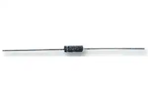
## Axial Lead Rectifiers
## **SCHOTTKY BARRIER RECTIFIERS 1.0 AMPERE 20, 30 and 40 VOLTS**
## 1N5817, 1N5818, 1N5819
This series employs the Schottky Barrier principle in a large area metal−to−silicon power diode. State−of−the−art geometry features chrome barrier metal, epitaxial construction with oxide passivation and metal overlap contact. Ideally suited for use as rectifiers in low−voltage, high−frequency inverters, free wheeling diodes, and polarity protection diodes.
**==> picture [49 x 27] intentionally omitted <==**
**----- Start of picture text -----**<br>
AXIAL LEAD<br>CASE 59<br>STYLE 1<br>**----- End of picture text -----**<br>
## **Features**
- Extremely Low VF
- Low Stored Charge, Majority Carrier Conduction
## **MARKING DIAGRAM**
- Low Power Loss/High Efficiency
- These are Pb−Free Devices*
## **Mechanical Characteristics:**
- Case: Epoxy, Molded
- Weight: 0.4 Gram (Approximately)
- Finish: All External Surfaces Corrosion Resistant and Terminal Leads are Readily Solderable
- Lead Temperature for Soldering Purposes: 260°C Max for 10 Seconds
- Polarity: Cathode Indicated by Polarity Band
- ESD Ratings: Machine Model = C (>400 V) Human Body Model = 3B (>8000 V)
**==> picture [41 x 42] intentionally omitted <==**
**----- Start of picture text -----**<br>
A<br>1N581x<br>YYWW �<br>�<br>**----- End of picture text -----**<br>
A =Assembly Location 1N581x =Device Number x= 7, 8, or 9 YY =Year WW =Work Week � =Pb−Free Package
(Note: Microdot may be in either location)
## **ORDERING INFORMATION**
See detailed ordering and shipping information on page 6 of this data sheet.
> *For additional information on our Pb−Free strategy and soldering details, please download the **onsemi** Soldering and Mounting Techniques Reference Manual, SOLDERRM/D.
Publication Order Number:
**1**
© Semiconductor Components Industries, LLC, 2006 **August, 2021 − Rev. 11**
**1N5817/D**
**1N5817, 1N5818, 1N5819**
## **MAXIMUM RATINGS**
|**MAXIMUM RATINGS**||||||
|---|---|---|---|---|---|
|**Rating**|**Symbol**|**1N5817**|**1N5818**|**1N5819**|**Unit**|
|Peak Repetitive Reverse Voltage<br>Working Peak Reverse Voltage<br>DC Blocking Voltage|VRRM<br>VRWM<br>VR|20|30|40|V|
|Non−Repetitive Peak Reverse Voltage|VRSM|24|36|48|V|
|RMS Reverse Voltage|VR(RMS)|14|21|28|V|
|Average Rectified Forward Current (Note 1), (VR(equiv) ≤0.2 VR(dc), TL= 90°C,<br>R�JA= 80°C/W, P.C. Board Mounting, see Note 2, TA= 55°C)|IO|1.0|||A|
|Ambient Temperature (Rated VR(dc), PF(AV)= 0, R�JA= 80°C/W)|TA|85|80|75|°C|
|Non−Repetitive Peak Surge Current, (Surge applied at rated load conditions,<br>half−wave, single phase 60 Hz, TL= 70°C)|IFSM|25 (for one cycle)|||A|
|Operating and Storage Junction Temperature Range (Reverse Voltage applied)|TJ, Tstg|−65 to +125|||°C|
|Peak Operating Junction Temperature (Forward Current applied)|TJ(pk)|150|||°C|
Stresses exceeding those listed in the Maximum Ratings table may damage the device. If any of these limits are exceeded, device functionality should not be assumed, damage may occur and reliability may be affected.
## **THERMAL CHARACTERISTICS** (Note 1)
|**THERMAL CHARACTERISTICS**(Note 1)||||||
|---|---|---|---|---|---|
|**Characteristic**|**Symbol**||**Max**||**Unit**|
|Thermal Resistance, Junction−to−Ambient|R�JA||80||°C/W|
|**ELECTRICAL CHARACTERISTICS**(TL= 25°C unless otherwise noted) (Note 1)||||||
|**Characteristic**|**Symbol**|**1N5817**|**1N5818**|**1N5819**|**Unit**|
|Maximum Instantaneous Forward Voltage (Note 2)<br>(iF= 0.1 A)<br>(iF= 1.0 A)<br>(iF= 3.0 A)|vF|0.32<br>0.45<br>0.75|0.33<br>0.55<br>0.875|0.34<br>0.6<br>0.9|V|
|Maximum Instantaneous Reverse Current @ Rated dc Voltage (Note 2)<br>(TL= 25°C)<br>(TL= 100°C)|IR|1.0<br>10|1.0<br>10|1.0<br>10|mA|
1. Lead Temperature reference is cathode lead 1/32 in from case.
2. Pulse Test: Pulse Width = 300 � s, Duty Cycle = 2.0%.
**www.onsemi.com**
**2**
**1N5817, 1N5818, 1N5819**
## **NOTE 3. — DETERMINING MAXIMUM RATINGS**
Reverse power dissipation and the possibility of thermal runaway must be considered when operating this rectifier at reverse voltages above 0.1 VRWM. Proper derating may be accomplished by use of equation (1).
**==> picture [229 x 80] intentionally omitted <==**
Figures 1, 2, and 3 permit easier use of equation (1) by taking reverse power dissipation and thermal runaway into consideration. The figures solve for a reference temperature as determined by equation (2).
**==> picture [155 x 10] intentionally omitted <==**
Substituting equation (2) into equation (1) yields:
**==> picture [163 x 10] intentionally omitted <==**
Inspection of equations (2) and (3) reveals that TR is the ambient temperature at which thermal runaway occurs or where TJ = 125°C, when forward power is zero. The transition from one boundary condition to the other is evident on the curves of Figures 1, 2, and 3 as a difference in the rate of change of the slope in the vicinity of 115°C. The data of Figures 1, 2, and 3 is based upon dc conditions. For use in common rectifier circuits, Table 1 indicates suggested factors for an equivalent dc voltage to use for conservative design, that is:
**==> picture [164 x 11] intentionally omitted <==**
The factor F is derived by considering the properties of the various rectifier circuits and the reverse characteristics of Schottky diodes.
EXAMPLE: Find TA(max) for 1N5818 operated in a 12−volt dc supply using a bridge circuit with capacitive filter such that IDC = 0.4 A (IF(AV) = 0.5 A), I(FM)/I(AV) = 10, Input Voltage = 10 V(rms), R�JA = 80°C/W.
Step 1. Find VR(equiv). Read F = 0.65 from Table 1, Step 1. Find ∴ VR(equiv) = (1.41)(10)(0.65) = 9.2 V. Step 2. Find TR from Figure 2. Read TR = 109 ° C Step 1. Find @ VR = 9.2 V and R � JA = 80 ° C/W.
Step 3. Find PF(AV) from Figure 4. **Read PF(AV) = 0.5 W
**==> picture [164 x 47] intentionally omitted <==**
**Values given are for the 1N5818. Power is slightly lower for the 1N5817 because of its lower forward voltage, and higher for the 1N5819.
**==> picture [243 x 169] intentionally omitted <==**
**----- Start of picture text -----**<br>
125<br>40 30 23<br>° 115<br>105<br>R�JA (°C/W) = 110<br>95<br>80<br>60<br>85<br>75<br>2.0 3.0 4.0 5.0 7.0 10 15 20<br>VR, DC REVERSE VOLTAGE (VOLTS)<br>C)<br>TR, REFERENCE TEMPERATURE (<br>**----- End of picture text -----**<br>
**Figure 1. Maximum Reference Temperature 1N5817**
**==> picture [244 x 360] intentionally omitted <==**
**----- Start of picture text -----**<br>
125<br>40 30 23<br>° 115<br>105<br>R�JA (°C/W) = 110<br>80<br>95 60<br>85<br>75<br>3.0 4.0 5.0 7.0 10 15 20 30<br>VR, DC REVERSE VOLTAGE (VOLTS)<br>Figure 2. Maximum Reference Temperature<br>1N5818<br>125<br>40<br>30<br>° 115 23<br>105 R�JA (°C/W) = 110<br>80<br>95<br>60<br>85<br>75<br>4.0 5.0 7.0 10 15 20 30 40<br>VR, DC REVERSE VOLTAGE (VOLTS)<br>C)<br>TR, REFERENCE TEMPERATURE (<br>C)<br>TR, REFERENCE TEMPERATURE (<br>**----- End of picture text -----**<br>
**Figure 3. Maximum Reference Temperature 1N5819**
**Table 1. Values for Factor F**
|**Circuit**|**Half Wave**|**Half Wave**|**Full Wave, Bridge**|**Full Wave, Bridge**|**Full Wave, Center Tapped*†**|**Full Wave, Center Tapped*†**|
|---|---|---|---|---|---|---|
|**Load**|**Resistive**|**Capacitive***|**Resistive**|**Capacitive**|**Resistive**|**Capacitive**|
|Sine Wave|0.5|1.3|0.5|0.65|1.0|1.3|
|Square Wave|0.75|1.5|0.75|0.75|1.5|1.5|
**Note that VR(PK) ≈ 2.0 Vin(PK).
†Use line to center tap voltage for Vin.
**www.onsemi.com**
**3**
**1N5817, 1N5818, 1N5819**
**==> picture [490 x 426] intentionally omitted <==**
**----- Start of picture text -----**<br>
90 5.0<br>Sine Wave<br>80 BOTH LEADS TO HEATSINK, 3.0 I (FM) = π (Resistive Load)<br>EQUAL LENGTH<br>2.0 I(AV)<br>70 5<br>Capacitive<br>10<br>60 1.0 Loads { dc<br>MAXIMUM 0.7 20<br>50 0.5 SQUARE WAVE<br>TYPICAL<br>40 0.3 TJ ≈ 125°C<br>0.2<br>30<br>0.1<br>20<br>0.07<br>10 0.05<br>1 1/8 1/4 3/8 1/2 5/8 3/4 7/8 1.0 0.2 0.4 0.6 0.8 1.0 2.0 4.0<br>L, LEAD LENGTH (INCHES) IF(AV), AVERAGE FORWARD CURRENT (AMP)<br>Figure 4. Steady−State Thermal Resistance Figure 5. Forward Power Dissipation<br>1N5817−19<br>1.0<br>0.7<br>0.5<br>0.3<br>Z�JL(t) = Z�JL • r(t)<br>0.2<br>P P<br>0.1 tp pk pk DUTY CYCLE, D = tPEAK POWER, P an pk , is peak ofp/t1<br>0.07 TIME equivalent square power pulse.<br>0.05 � TJL = Ppk • R �t JL 1 [D + (1 − D) • r(t1 + tp) + r(tp) − r(t1)] where<br>0.03 � T JL = the increase in junction temperature above the lead temperature<br>r(t) = normalized value of transient thermal resistance at time, t, from Figure 6,<br>0.02 i.e.:<br>r(t) = r(t 1 + t p ) = normalized value of transient thermal resistance at time, t 1 + t p .<br>0.01<br>0.1 0.2 0.5 1.0 2.0 5.0 10 20 50 100 200 500 1.0k 2.0k 5.0k 10k<br>t, TIME (ms)<br>C/W)°<br>PF(AV), AVERAGE POWER DISSIPATION (WATTS)<br>JL, THERMAL RESISTANCE, JUNCTION-TO-LEAD (<br>θ<br>R<br>r(t), TRANSIENT THERMAL RESISTANCE (NORMALIZED)<br>**----- End of picture text -----**<br>
**Figure 6. Thermal Response**
## **NOTE 4. — MOUNTING DATA**
Data shown for thermal resistance, junction−to−ambient (R�JA) for the mountings shown is to be used as typical guideline values for preliminary engineering, or in case the tie point temperature cannot be measured.
## **TYPICAL VALUES FOR R** � **JA IN STILL AIR**
||**1/8**|**1/4**|**1/2**|**3/4**|**3/4**|
|---|---|---|---|---|---|
|**1**|52|65|72|85|°C/W|
|2|67|80|87|100|°C/W|
|3|50||||°C/W|
**==> picture [230 x 186] intentionally omitted <==**
**----- Start of picture text -----**<br>
Mounting Method 1 Mounting Method 3<br>P.C. Board with P.C. Board with<br>1−1/2 ″ x 1−1/2 ″ 1−1/2 ″ x 1−1/2 ″<br>copper surface. copper surface.<br>L = 3/8″<br>L L<br>BOARD GROUND<br>PLANE<br>Mounting Method 2<br>L L<br>VECTOR PIN MOUNTING<br>**----- End of picture text -----**<br>
**www.onsemi.com**
**4**
**1N5817, 1N5818, 1N5819**
**NOTE 5. — THERMAL CIRCUIT MODEL**
(For heat conduction through the leads)
**==> picture [214 x 74] intentionally omitted <==**
**----- Start of picture text -----**<br>
R�S(A) R�L(A) R�J(A) R�J(K) R�L(K) R�S(K)<br>TA(A) PD TA(K)<br>TL(A) TC(A) TJ TC(K) TL(K)<br>**----- End of picture text -----**<br>
Use of the above model permits junction to lead thermal resistance for any mounting configuration to be found. For a given total lead length, lowest values occur when one side of the rectifier is brought as close as possible to the heatsink. Terms in the model signify:
(Subscripts A and K refer to anode and cathode sides, respectively.) Values for thermal resistance components are: R � L = 100 ° C/W/in typically and 120 ° C/W/in maximum R � J = 36 ° C/W typically and 46 ° C/W maximum.
TA = Ambient Temperature TC = Case Temperature TL = Lead Temperature TJ = Junction Temperature
R � S = Thermal Resistance, Heatsink to Ambient
R � L = Thermal Resistance, Lead to Heatsink
R � J = Thermal Resistance, Junction to Case PD = Power DissipationD = Power Dissipation = Power Dissipation
**==> picture [485 x 377] intentionally omitted <==**
**----- Start of picture text -----**<br>
PD = Power DissipationD = Power Dissipation = Power Dissipation 30<br>20<br>20 1 Cycle<br>TL = 70 ° C<br>f = 60 Hz<br>10<br>10<br>7.0<br>5.0 TC = 100 ° C 7.0<br>5.0<br>3.0<br>Surge Applied at<br>2.0 Rated Load Conditions<br>25°C 3.0<br>1.0 2.0 3.0 5.0 7.0 10 20 30 40 70 100<br>NUMBER OF CYCLES<br>1.0<br>0.7 Figure 8. Maximum Non−Repetitive Surge Current<br>0.5<br>3020 TJ = 125 ° C<br>0.3<br>15<br>0.2 100°C<br>5.0<br>3.0<br>2.0<br>0.1 75 ° C<br>1.0<br>0.07<br>0.5<br>0.05 0.3 25°C<br>0.2<br>0.03 0.1 1N5817<br>1N5818<br>0.02 0.05<br>0.1 0.2 0.3 0.4 0.5 0.6 0.7 0.8 0.9 1.0 1.1 0.03 1N5819<br>vF, INSTANTANEOUS FORWARD VOLTAGE (VOLTS) 0 4.0 8.0 12 16 20 24 28 32 36 40<br>VR, REVERSE VOLTAGE (VOLTS)<br>IFSM, PEAK SURGE CURRENT (AMP)<br>iF, INSTANTANEOUS FORWARD CURRENT (AMP)<br>IR, REVERSE CURRENT (mA)<br>**----- End of picture text -----**<br>
**Figure 9. Typical Reverse Current**
**Figure 7. Typical Forward Voltage**
**www.onsemi.com**
**5**
**1N5817, 1N5818, 1N5819**
## **NOTE 6. — HIGH FREQUENCY OPERATION**
Since current flow in a Schottky rectifier is the result of majority carrier conduction, it is not subject to junction diode forward and reverse recovery transients due to minority carrier injection and stored charge. Satisfactory circuit analysis work may be performed by using a model consisting of an ideal diode in parallel with a variable capacitance. (See Figure 10.)
Rectification efficiency measurements show that operation will be satisfactory up to several megahertz. For example, relative waveform rectification efficiency is approximately 70 percent at 2.0 MHz, e.g., the ratio of dc power to RMS power in the load is 0.28 at this frequency, whereas perfect rectification would yield 0.406 for sine wave inputs. However, in contrast to ordinary junction diodes, the loss in waveform efficiency is not indicative of power loss: it is simply a result of reverse current flow through the diode capacitance, which lowers the dc output voltage.
**==> picture [239 x 166] intentionally omitted <==**
**----- Start of picture text -----**<br>
200<br>100<br>1N5817<br>70<br>1N5818<br>50<br>1N5819<br>30<br>TJ = 25 ° C<br>20 f = 1.0 MHz<br>10<br>0.4 0.6 0.8 1.0 2.0 4.0 6.0 8.0 10 20 40<br>VR, REVERSE VOLTAGE (VOLTS)<br>C, CAPACITANCE (pF)<br>**----- End of picture text -----**<br>
**Figure 10. Typical Capacitance**
## **ORDERING INFORMATION**
|**ORDERING INFORMATION**|||
|---|---|---|
|**Device**|**Package**|**Shipping**†|
|1N5817|Axial Lead*|1000 Units / Bag|
|1N5817G|Axial Lead*|1000 Units / Bag|
|1N5817RL|Axial Lead*|5000 / Tape & Reel|
|1N5817RLG|Axial Lead*|5000 / Tape & Reel|
|1N5818|Axial Lead*|1000 Units / Bag|
|1N5818G|Axial Lead*|1000 Units / Bag|
|1N5818RL|Axial Lead*|5000 / Tape & Reel|
|1N5818RLG|Axial Lead*|5000 / Tape & Reel|
|1N5819|Axial Lead*|1000 Units / Bag|
|1N5819G|Axial Lead*|1000 Units / Bag|
|1N5819RL|Axial Lead*|5000 / Tape & Reel|
|1N5819RLG|Axial Lead*|5000 / Tape & Reel|
†For information on tape and reel specifications, including part orientation and tape sizes, please refer to our Tape and Reel Packaging Specifications Brochure, BRD8011/D.
*This package is inherently Pb−Free.
**www.onsemi.com**
**6**
MECHANICAL CASE OUTLINE **PACKAGE DIMENSIONS**
**==> picture [451 x 350] intentionally omitted <==**
**----- Start of picture text -----**<br>
AXIAL LEAD<br>CASE 59−10<br>ISSUE U<br>DATE 15 FEB 2005<br>B<br>NOTES:<br>1. DIMENSIONING AND TOLERANCING PER ANSI<br>Y14.5M, 1982.<br>2. CONTROLLING DIMENSION: INCH.<br>K D 3. ALL RULES AND NOTES ASSOCIATED WITHJEDEC DO−41 OUTLINE SHALL APPLY<br>STYLE 1 STYLE 2 4. POLARITY DENOTED BY CATHODE BAND.<br>F 5. LEAD DIAMETER NOT CONTROLLED WITHIN F<br>DIMENSION.<br>A INCHES MILLIMETERS<br>DIM MIN MAX MIN MAX<br>A 0.161 0.205 4.10 5.20<br>SCALE 1:1 OPTIONAL AS NEEDEDPOLARITY INDICATOR(SEE STYLES) F BD 0.0790.028 0.1060.034 2.000.71 2.700.86<br>F −−− 0.050 −−− 1.27<br>K K 1.000 −−− 25.40 −−−<br>GENERIC<br>te| MARKING DIAGRAM*<br> A A<br>STYLE 1: STYLE 2: xxx xxx<br>PIN 1. CATHODE (POLARITY BAND) NO POLARITY<br>2. ANODE xxx xxx<br>4( YYWW GH6G YYWW<br>STYLE 1 STYLE 2<br>xxx = Specific Device Code<br>A = Assembly Location<br>YY = Year<br>WW = Work Week<br>**----- End of picture text -----**<br>
**==> picture [159 x 36] intentionally omitted <==**
**----- Start of picture text -----**<br>
*This information is generic. Please refer to<br>device data sheet for actual part marking.<br>Pb−Free indicator, “G” or microdot “ ”,<br>may or may not be present.<br>**----- End of picture text -----**<br>
Electronic versions are uncontrolled except when accessed directly from the Document Repository. **DOCUMENT NUMBER: 98ASB42045B** Printed versions are uncontrolled except when stamped “CONTROLLED COPY” in red. **DESCRIPTION: AXIAL LEAD PAGE 1 OF 1** ~~[| aT~~ ON Semiconductor and are trademarks of Semiconductor Components Industries, LLC dba ON Semiconductor or its subsidiaries in the United States and/or other countries. ON Semiconductor reserves the right to make changes without further notice to any products herein. ON Semiconductor makes no warranty, representation or guarantee regarding the suitability of its products for any particular purpose, nor does ON Semiconductor assume any liability arising out of the application or use of any product or circuit, and specifically disclaims any and all liability, including without limitation special, consequential or incidental damages. ON Semiconductor does not convey any license under its patent rights nor the rights of others.
Electronic versions are uncontrolled except when accessed directly from the Document Repository. Printed versions are uncontrolled except when stamped “CONTROLLED COPY” in red.
www.onsemi.com
© Semiconductor Components Industries, LLC, 2019
**onsemi** , , and other names, marks, and brands are registered and/or common law trademarks of Semiconductor Components Industries, LLC dba “ **onsemi** ” or its affiliates and/or subsidiaries in the United States and/or other countries. **onsemi** owns the rights to a number of patents, trademarks, copyrights, trade secrets, and other intellectual property. A listing of **onsemi** ’s product/patent coverage may be accessed at www.onsemi.com/site/pdf/Patent−Marking.pdf. **onsemi** reserves the right to make changes at any time to any products or information herein, without notice. The information herein is provided “as−is” and **onsemi** makes no warranty, representation or guarantee regarding the accuracy of the information, product features, availability, functionality, or suitability of its products for any particular purpose, nor does **onsemi** assume any liability arising out of the application or use of any product or circuit, and specifically disclaims any and all liability, including without limitation special, consequential or incidental damages. Buyer is responsible for its products and applications using **onsemi** products, including compliance with all laws, regulations and safety requirements or standards, regardless of any support or applications information provided by **onsemi** . “Typical” parameters which may be provided in **onsemi** data sheets and/or specifications can and do vary in different applications and actual performance may vary over time. All operating parameters, including “Typicals” must be validated for each customer application by customer’s technical experts. **onsemi** does not convey any license under any of its intellectual property rights nor the rights of others. **onsemi** products are not designed, intended, or authorized for use as a critical component in life support systems or any FDA Class 3 medical devices or medical devices with a same or similar classification in a foreign jurisdiction or any devices intended for implantation in the human body. Should Buyer purchase or use **onsemi** products for any such unintended or unauthorized application, Buyer shall indemnify and hold **onsemi** and its officers, employees, subsidiaries, affiliates, and distributors harmless against all claims, costs, damages, and expenses, and reasonable attorney fees arising out of, directly or indirectly, any claim of personal injury or death associated with such unintended or unauthorized use, even if such claim alleges that **onsemi** was negligent regarding the design or manufacture of the part. **onsemi** is an Equal Opportunity/Affirmative Action Employer. This literature is subject to all applicable copyright laws and is not for resale in any manner.
## **PUBLICATION ORDERING INFORMATION**
**LITERATURE FULFILLMENT** : **TECHNICAL SUPPORT Email Requests to:** orderlit@onsemi.com **North American Technical Support: Europe, Middle East and Africa Technical Support:** Voice Mail: 1 800−282−9855 Toll Free USA/Canada Phone: 00421 33 790 2910 **onsemi Website:** www.onsemi.com Phone: 011 421 33 790 2910 For additional information, please contact your local Sales Representative
◊
**==> picture [232 x 43] intentionally omitted <==**
Updated at June 4, 2026
onsemi is a premier global supplier of intelligent power and sensing technologies, driving disruptive innovations across the automotive, industrial, and cloud infrastructure markets. Recognized for their commitment to sustainability and reliable supply chains, the company accelerates advancements in vehicle electrification, industrial automation, and 5G networks by solving the industry's most complex design challenges. At the core of their portfolio is an industry-leading selection of discrete semiconductors. This extensive range features thousands of high-performance bipolar transistors, single and dual MOSFETs, and a comprehensive array of diodes, including Zener, Schottky, and fast-recovery rectifiers. Engineered for superior thermal performance and energy efficiency, these foundational components are critical for demanding power conversion, switching, and signal conditioning applications. Beyond essential discretes, onsemi provides a robust suite of advanced power management and circuit protection solutions. Their lineup includes intelligent power modules, single IGBTs, and transient voltage suppression (TVS) diodes designed to safeguard sensitive circuitry. Complimented by integrated passive filters, AC/DC LED driver ICs, and specialized sub-2.4GHz RF transceivers, onsemi equips engineers with the scalable, high-quality technologies needed to build a cleaner, smarter, and more connected world.
About Novapart
Novapart is a B2B electronic component broker specialising in stock shortages and cost reduction. We source hard-to-find parts and identify compliant alternatives across a catalogue of 410,000+ components from 500+ manufacturers.
Learn more →Stock Shortage Specialist
When a component is unavailable, discontinued or has an unacceptable lead time, we tap into our network of vetted European and Asian distributors to source what you need — without compromising on quality or traceability.
Request a quote →Compliant Alternatives
We identify pin-to-pin, electrically equivalent substitutes that meet the same certifications (RoHS, AEC-Q100, REACH) as your original specification — validated against datasheets, not just part numbers. Often at a lower cost.
BOM Analysis service →