
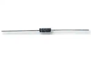


1N5360BG
Zener Single Diode, 25 V, 5 W, 017AA, 2 Pins, 200 °C, Through Hole
- Manufacturer: ONSEMI
- Product type: Zener Single Diodes
- Zener Voltage Vz Typ:25V; Power Dissipation Pd:5W; Diode Case Style:017AA; Zener Tolerance ±:5%; No. of Pins:2Pins; Operating Temperature Max:200°C; Product Range:1N53 Series; Automotive Qualificat
- SVHC: Lead (25-Jun-2025)
- No. of Pins: 2Pins
- Product Range: 1N53 Series
- Qualification: -
- Diode Mounting: Through Hole
- Diode Case Style: 017AA
- Power Dissipation: 5W
- Zener Voltage Nom: 25V
- Operating Temperature Max: 200°C
| Delivery and price | |
|---|---|
| Units per pack | 5000 |
| Price | 0.115 € |
| Current stock | 1000+ |
| Lead time | 30 days |
## 1N53 Series

## @

## 5 Watt Surmetic 40 Zener Voltage Regulators

This is a complete series of 5 Watt Zener diodes with tight limits and better operating characteristics that reflect the superior capabilities of silicon−oxide passivated junctions. All this in an axial lead, transfer−molded plastic package that offers protection in all common environmental conditions.

**http://onsemi.com**

## **Features**

Cathode Anode

- Zener Voltage Range − 3.3 V to 200 V

- ESD Rating of Class 3 (>16 kV) per Human Body Model

**AXIAL LEAD CASE 017AA** ~~a~~ **PLASTIC**

- Surge Rating of up to 180 W @ 8.3 ms

- Maximum Limits Guaranteed on up to Six Electrical Parameters

- Pb−Free Packages are Available*

## **Mechanical Characteristics**

**CASE:** Void free, transfer−molded, thermosetting plastic **FINISH:** All external surfaces are corrosion resistant and leads are readily solderable

## **MARKING DIAGRAM**

**MAXIMUM LEAD TEMPERATURE FOR SOLDERING PURPOSES:** 260°C, 1/16 in. from the case for 10 seconds **POLARITY:** Cathode indicated by polarity band **MOUNTING POSITION:** Any

A 1N 53xxB YYWW ~~S[k~~ A = Assembly Location 1N53xxB = Device Number (Refer to Tables on Pages 3 & 4) YY = Year WW = Work Week = Pb−Free Package (Note: Microdot may be in either location)

## **MAXIMUM RATINGS**

**Rating Symbol Value Unit** Max. Steady State Power Dissipation PD 5 W @ TL = 25 ° C, Lead Length = 3/8 in Derate above 25 ° C 40 mW/ ° C Junction−to−Lead Thermal Resistance JL 25 ° C/W ~~T_T).~~ Operating and Storage TJ, Tstg −65 to +200 ° C Temperature Range (Note 1) ~~PC~~ Stresses exceeding Maximum Ratings may damage the device. Maximum Ratings are stress ratings only. Functional operation above the Recommended Operating Conditions is not implied. Extended exposure to stresses above the Recommended Operating Conditions may affect device reliability.

**ORDERING INFORMATION**

**Device Package Shipping**[†] 1N53xxB, G Axial Lead 1000 Units/Box (Pb−Free) 1N53xxBRL, G Axial Lead 4000/Tape & Reel (Pb−Free) ~~++~~ †For information on tape and reel specifications, ~~—~~ including part orientation and tape sizes, please refer to our Tape and Reel Packaging Specifications Brochure, BRD8011/D.

1. Max operating temperature for DC conditions is 150 ° C, but not to exceed 200 ° C for pulsed conditions with low duty cycle or non−repetitive.

> *For additional information on our Pb−Free strategy and soldering details, please download the ON Semiconductor Soldering and Mounting Techniques Reference Manual, SOLDERRM/D.

Publication Order Number:

**1**

© Semiconductor Components Industries, LLC, 2013 **November, 2013 − Rev. 15**

**1N5333B/D**

**1N53 Series**

## **ELECTRICAL CHARACTERISTICS** (TA = 25 ° C unless

otherwise noted, VF = 1.2 V Max @ IF = 1.0 A for all types)

|otherwise n|oted, VF= 1.2 V Max @ IF= 1.0 A for all types)|
|---|---|
|**Symbol**|**Parameter**|
|VZ|Reverse Zener Voltage @ IZT|
|IZT|Reverse Current|
|ZZT|Maximum Zener Impedance @ IZT|
|IZK|Reverse Current|
|ZZK|Maximum Zener Impedance @ IZK|
|IR|Reverse Leakage Current @ VR|
|VR|Breakdown Voltage|
|IF|Forward Current|
|VF|Forward Voltage @ IF|
|IR|Maximum Surge Current @ TA= 25°C|
|�VZ|Reverse Zener Voltage Change|
|IZM|Maximum DC Zener Current|


**==> picture [194 x 197] intentionally omitted <==**

**----- Start of picture text -----**<br>
I<br>IF<br>VZ VR V<br>IR VF<br>IZT<br>Zener Voltage Regulator<br>**----- End of picture text -----**<br>


## **ELECTRICAL CHARACTERISTICS** (TA = 25 ° C unless otherwise noted, VF = 1.2 V Max @ IF = 1.0 A for all types)

|**Device**†<br>(Note 2)|**Device**<br>**Marking**|**Zener Voltage**(Note 3)|**Zener Voltage**(Note 3)|**Zener Voltage**(Note 3)|**Zener Voltage**(Note 3)|**Zener Impedance**(Note 3)|**Zener Impedance**(Note 3)|**Zener Impedance**(Note 3)|**Leakage**<br>**Current**|**Leakage**<br>**Current**|**IR**<br>(Note 4)|**�VZ**<br>(Note 5)|**IZM**<br>(Note 6)|
|---|---|---|---|---|---|---|---|---|---|---|---|---|---|
|||**VZ (Volts)**|||**@ IZT**|**ZZT @ IZT**|**ZZK @ IZK**|**IZK**|**IR @**|**VR**||||
|||**Min**|**Nom**|**Max**|**mA**|**�**|**�**|**mA**|�**A Max**|**Volts**|**A**|**Volts**|**mA**|
|**_1N5333B_**<br>1N5334B<br>1N5335B<br>1N5336B<br>**_1N5337B_**|**_1N5333B_**<br>1N5334B<br>1N5335B<br>1N5336B<br>**_1N5337B_**|**_3.14_**<br>3.42<br>3.71<br>4.09<br>**_4.47_**|**_3.3_**<br>3.6<br>3.9<br>4.3<br>**_4.7_**|**_3.47_**<br>3.78<br>4.10<br>4.52<br>**_4.94_**|**_380_**<br>350<br>320<br>290<br>**_260_**|**_3_**<br>2.5<br>2<br>2<br>**_2_**|**_400_**<br>500<br>500<br>500<br>**_450_**|**_1_**<br>1<br>1<br>1<br>**_1_**|**_300_**<br>150<br>50<br>10<br>**_5_**|**_1_**<br>1<br>1<br>1<br>**_1_**|**_20_**<br>18.7<br>17.6<br>16.4<br>**_15.3_**|**_0.85_**<br>0.8<br>0.54<br>0.49<br>**_0.44_**|**_1440_**<br>1320<br>1220<br>1100<br>**_1010_**|
|**_1N5338B_**<br>**_1N5339B_**<br>1N5340B<br>**_1N5341B_**<br>**_1N5342B_**|**_1N5338B_**<br>**_1N5339B_**<br>1N5340B<br>**_1N5341B_**<br>**_1N5342B_**|**_4.85_**<br>**_5.32_**<br>5.70<br>**_5.89_**<br>**_6.46_**|**_5.1_**<br>**_5.6_**<br>6.0<br>**_6.2_**<br>**_6.8_**|**_5.36_**<br>**_5.88_**<br>6.30<br>**_6.51_**<br>**_7.14_**|**_240_**<br>**_220_**<br>200<br>**_200_**<br>**_175_**|**_1.5_**<br>**_1_**<br>1<br>**_1_**<br>**_1_**|**_400_**<br>**_400_**<br>300<br>**_200_**<br>**_200_**|**_1_**<br>**_1_**<br>1<br>**_1_**<br>**_1_**|**_1_**<br>**_1_**<br>1<br>**_1_**<br>**_10_**|**_1_**<br>**_2_**<br>3<br>**_3_**<br>**_5.2_**|**_14.4_**<br>**_13.4_**<br>12.7<br>**_12.4_**<br>**_11.5_**|**_0.39_**<br>**_0.25_**<br>0.19<br>**_0.1_**<br>**_0.15_**|**_930_**<br>**_865_**<br>790<br>**_765_**<br>**_700_**|
|1N5343B<br>1N5344B<br>1N5345B<br>1N5346B<br>**_1N5347B_**|1N5343B<br>1N5344B<br>1N5345B<br>1N5346B<br>**_1N5347B_**|7.13<br>7.79<br>8.27<br>8.65<br>**_9.50_**|7.5<br>8.2<br>8.7<br>9.1<br>**_10_**|7.88<br>8.61<br>9.14<br>9.56<br>**_10.5_**|175<br>150<br>150<br>150<br>**_125_**|1.5<br>1.5<br>2<br>2<br>**_2_**|200<br>200<br>200<br>150<br>**_125_**|1<br>1<br>1<br>1<br>**_1_**|10<br>10<br>10<br>7.5<br>**_5_**|5.7<br>6.2<br>6.6<br>6.9<br>**_7.6_**|10.7<br>10<br>9.5<br>9.2<br>**_8.6_**|0.15<br>0.2<br>0.2<br>0.22<br>**_0.22_**|630<br>580<br>545<br>520<br>**_475_**|


Devices listed in _**bold, italic**_ are ON Semiconductor **Preferred** devices. **Preferred** devices are recommended choices for future use and best overall value.

2. **TOLERANCE AND TYPE NUMBER DESIGNATION:** The JEDEC type numbers shown indicate a tolerance of ± 5%.

3. **ZENER VOLTAGE (VZ) and IMPEDANCE (IZT and IZK):** Test conditions for zener voltage and impedance are as follows: IZ is applied 40 ± 10 ms prior to reading. Mounting contacts are located 3/8 ″ to 1/2 ″ from the inside edge of mounting clips to the body of the diode (TA = 25 ° C +8 ° C, −2 ° C).

4. **SURGE CURRENT (IR):** Surge current is specified as the maximum allowable peak, non−recurrent square−wave current with a pulse width, PW, of 8.3 ms. The data given in Figure 5 may be used to find the maximum surge current for a square wave of any pulse width between 1 ms and 1000 ms by plotting the applicable points on logarithmic paper. Examples of this, using the 3.3 V and 200 V zener are shown in Figure 6. Mounting contact located as specified in Note 2 (TA = 25 ° C +8 ° C, −2 ° C).

5. **VOLTAGE REGULATION ( � VZ):** The conditions for voltage regulation are as follows: VZ measurements are made at 10% and then at 50% of the IZ max value listed in the electrical characteristics table. The test current time duration for each VZ measurement is 40 ± 10 ms. Mounting contact located as specified in Note 2 (TA = 25 ° C +8 ° C, −2 ° C).

6. **MAXIMUM REGULATOR CURRENT (IZM):** The maximum current shown is based on the maximum voltage of a 5% type unit, therefore, it applies only to the B−suffix device. The actual IZM for any device may not exceed the value of 5 watts divided by the actual VZ of the device. TL = 25 ° C at 3/8 ″ maximum from the device body.

- †The “G’’ suffix indicates Pb−Free package or Pb−Free packages are available.

**http://onsemi.com**

**2**

## **1N53 Series**

**ELECTRICAL CHARACTERISTICS** (TA = 25 ° C unless otherwise noted, VF = 1.2 V Max @ IF = 1.0 A for all types)

|**Device**†<br>(Note 7)|**Device**<br>**Marking**|**Zener Voltage**(Note 8)|**Zener Voltage**(Note 8)|**Zener Voltage**(Note 8)|**Zener Voltage**(Note 8)|**Zener Impedance**(Note 8)|**Zener Impedance**(Note 8)|**Zener Impedance**(Note 8)|**Leakage**<br>**Current**|**Leakage**<br>**Current**|**IR**<br>(Note 9)|**�VZ**<br>(Note<br>10)|**IZM**<br>(Note 11)|
|---|---|---|---|---|---|---|---|---|---|---|---|---|---|
|||**VZ (Volts)**|||**@ IZT**|**ZZT @ IZT**|**ZZK @ IZK**|**IZK**|**IR @**|**VR**||||
|||**Min**|**Nom**|**Max**|**mA**|**�**|**�**|**mA**|�**A Max**|**Volts**|**A**|**Volts**|**mA**|
|1N5348B<br>**_1N5349B_**<br>**_1N5350B_**<br>1N5351B<br>**_1N5352B_**|1N5348B<br>**_1N5349B_**<br>**_1N5350B_**<br>1N5351B<br>**_1N5352B_**|10.45<br>**_11.4_**<br>**_12.35_**<br>13.3<br>**_14.25_**|11<br>**_12_**<br>**_13_**<br>14<br>**_15_**|11.55<br>**_12.6_**<br>**_13.65_**<br>14.7<br>**_15.75_**|125<br>**_100_**<br>**_100_**<br>100<br>**_75_**|2.5<br>**_2.5_**<br>**_2.5_**<br>2.5<br>**_2.5_**|125<br>**_125_**<br>**_100_**<br>75<br>**_75_**|1<br>**_1_**<br>**_1_**<br>1<br>**_1_**|5<br>**_2_**<br>**_1_**<br>1<br>**_1_**|8.4<br>**_9.1_**<br>**_9.9_**<br>10.6<br>**_11.5_**|8.0<br>**_7.5_**<br>**_7.0_**<br>6.7<br>**_6.3_**|0.25<br>**_0.25_**<br>**_0.25_**<br>0.25<br>**_0.25_**|430<br>**_395_**<br>**_365_**<br>340<br>**_315_**|
|**_1N5353B_**<br>1N5354B<br>1N5355B<br>1N5356B<br>1N5357B|**_1N5353B_**<br>1N5354B<br>1N5355B<br>1N5356B<br>1N5357B|**_15.2_**<br>16.15<br>17.1<br>18.05<br>19|**_16_**<br>17<br>18<br>19<br>20|**_16.8_**<br>17.85<br>18.9<br>19.95<br>21|**_75_**<br>70<br>65<br>65<br>65|**_2.5_**<br>2.5<br>2.5<br>3<br>3|**_75_**<br>75<br>75<br>75<br>75|**_1_**<br>1<br>1<br>1<br>1|**_1_**<br>0.5<br>0.5<br>0.5<br>0.5|**_12.2_**<br>12.9<br>13.7<br>14.4<br>15.2|**_6.0_**<br>5.8<br>5.5<br>5.3<br>5.1|**_0.3_**<br>0.35<br>0.4<br>0.4<br>0.4|**_295_**<br>280<br>264<br>250<br>237|
|**_1N5358B_**<br>**_1N5359B_**<br>1N5360B<br>**_1N5361B_**<br>1N5362B|**_1N5358B_**<br>**_1N5359B_**<br>1N5360B<br>**_1N5361B_**<br>1N5362B|**_20.9_**<br>**_22.8_**<br>23.75<br>**_25.65_**<br>26.6|**_22_**<br>**_24_**<br>25<br>**_27_**<br>28|**_23.1_**<br>**_25.2_**<br>26.25<br>**_28.35_**<br>29.4|**_50_**<br>**_50_**<br>50<br>**_50_**<br>50|**_3.5_**<br>**_3.5_**<br>4<br>**_5_**<br>6|**_75_**<br>**_100_**<br>110<br>**_120_**<br>130|**_1_**<br>**_1_**<br>1<br>**_1_**<br>1|**_0.5_**<br>**_0.5_**<br>0.5<br>**_0.5_**<br>0.5|**_16.7_**<br>**_18.2_**<br>19<br>**_20.6_**<br>21.2|**_4.7_**<br>**_4.4_**<br>4.3<br>**_4.1_**<br>3.9|**_0.45_**<br>**_0.55_**<br>0.55<br>**_0.6_**<br>0.6|**_216_**<br>**_198_**<br>190<br>**_176_**<br>170|
|1N5363B<br>1N5364B<br>**_1N5365B_**<br>1N5366B<br>1N5367B|1N5363B<br>1N5364B<br>**_1N5365B_**<br>1N5366B<br>1N5367B|28.5<br>31.35<br>**_34.2_**<br>37.05<br>40.85|30<br>33<br>**_36_**<br>39<br>43|31.5<br>34.65<br>**_37.8_**<br>40.95<br>45.15|40<br>40<br>**_30_**<br>30<br>30|8<br>10<br>**_11_**<br>14<br>20|140<br>150<br>**_160_**<br>170<br>190|1<br>1<br>**_1_**<br>1<br>1|0.5<br>0.5<br>**_0.5_**<br>0.5<br>0.5|22.8<br>25.1<br>**_27.4_**<br>29.7<br>32.7|3.7<br>3.5<br>**_3.5_**<br>3.1<br>2.8|0.6<br>0.6<br>**_0.65_**<br>0.65<br>0.7|158<br>144<br>**_132_**<br>122<br>110|
|**_1N5368B_**<br>1N5369B<br>1N5370B<br>1N5371B<br>1N5372B|**_1N5368B_**<br>1N5369B<br>1N5370B<br>1N5371B<br>1N5372B|**_44.65_**<br>48.45<br>53.2<br>57<br>58.9|**_47_**<br>51<br>56<br>60<br>62|**_49.35_**<br>53.55<br>58.8<br>63<br>65.1|**_25_**<br>25<br>20<br>20<br>20|**_25_**<br>27<br>35<br>40<br>42|**_210_**<br>230<br>280<br>350<br>400|**_1_**<br>1<br>1<br>1<br>1|**_0.5_**<br>0.5<br>0.5<br>0.5<br>0.5|**_35.8_**<br>38.8<br>42.6<br>45.5<br>47.1|**_2.7_**<br>2.5<br>2.3<br>2.2<br>2.1|**_0.8_**<br>0.9<br>1.0<br>1.2<br>1.35|**_100_**<br>93<br>86<br>79<br>76|
|1N5373B<br>1N5374B<br>1N5375B<br>1N5377B|1N5373B<br>1N5374B<br>1N5375B<br>1N5377B|64.6<br>71.25<br>77.9<br>86.45|68<br>75<br>82<br>91|71.4<br>78.75<br>86.1<br>95.55|20<br>20<br>15<br>15|44<br>45<br>65<br>75|500<br>620<br>720<br>760|1<br>1<br>1<br>1|0.5<br>0.5<br>0.5<br>0.5|51.7<br>56<br>62.2<br>69.2|2.0<br>1.9<br>1.8<br>1.6|1.52<br>1.6<br>1.8<br>2.2|70<br>63<br>58<br>52.5|
|1N5378B<br>1N5380B<br>1N5381B|1N5378B<br>1N5380B<br>1N5381B|95<br>114<br>123.5|100<br>120<br>130|105<br>126<br>136.5|12<br>10<br>10|90<br>170<br>190|800<br>1150<br>1250|1<br>1<br>1|0.5<br>0.5<br>0.5|76<br>91.2<br>98.8|1.5<br>1.3<br>1.2|2.5<br>2.5<br>2.5|47.5<br>39.5<br>36.6|
|**_1N5383B_**<br>1N5384B<br>1N5386B<br>1N5387B<br>1N5388B|**_1N5383B_**<br>1N5384B<br>1N5386B<br>1N5387B<br>1N5388B|**_142.5_**<br>152<br>171<br>180.5<br>190|**_150_**<br>160<br>180<br>190<br>200|**_157.5_**<br>168<br>189<br>199.5<br>210|**_8_**<br>8<br>5<br>5<br>5|**_330_**<br>350<br>430<br>450<br>480|**_1500_**<br>1650<br>1750<br>1850<br>1850|**_1_**<br>1<br>1<br>1<br>1|**_0.5_**<br>0.5<br>0.5<br>0.5<br>0.5|**_114_**<br>122<br>137<br>144<br>152|**_1.1_**<br>1.1<br>1.0<br>0.9<br>0.9|**_3.0_**<br>3.0<br>4.0<br>5.0<br>5.0|**_31.6_**<br>29.4<br>26.4<br>25<br>23.6|


Devices listed in _**bold, italic**_ are ON Semiconductor **Preferred** devices. **Preferred** devices are recommended choices for future use and best overall value.

7. **TOLERANCE AND TYPE NUMBER DESIGNATION:** The JEDEC type numbers shown indicate a tolerance of ± 5%.

8. **ZENER VOLTAGE (VZ) and IMPEDANCE (IZT and IZK):** Test conditions for zener voltage and impedance are as follows: IZ is applied 40 ± 10 ms prior to reading. Mounting contacts are located 3/8 ″ to 1/2 ″ from the inside edge of mounting clips to the body of the diode (TA = 25 ° C +8 ° C, −2 ° C).

9. **SURGE CURRENT (IR):** Surge current is specified as the maximum allowable peak, non−recurrent square−wave current with a pulse width, PW, of 8.3 ms. The data given in Figure 5 may be used to find the maximum surge current for a square wave of any pulse width between 1 ms and 1000 ms by plotting the applicable points on logarithmic paper. Examples of this, using the 3.3 V and 200 V zener are shown in Figure 6. Mounting contact located as specified in Note 7 (TA = 25 ° C +8 ° C, −2 ° C).

10. **VOLTAGE REGULATION ( � VZ):** The conditions for voltage regulation are as follows: VZ measurements are made at 10% and then at 50% of the IZ max value listed in the electrical characteristics table. The test current time duration for each VZ measurement is 40 ± 10 ms. Mounting contact located as specified in Note 7 (TA = 25 ° C +8 ° C, −2 ° C).

11. **MAXIMUM REGULATOR CURRENT (IZM):** The maximum current shown is based on the maximum voltage of a 5% type unit, therefore, it applies only to the B−suffix device. The actual IZM for any device may not exceed the value of 5 watts divided by the actual VZ of the device. TL = 25 ° C at 3/8 ″ maximum from the device body.

- †The “G’’ suffix indicates Pb−Free package or Pb−Free packages are available.

**http://onsemi.com**

**3**

**1N53 Series**

**==> picture [242 x 176] intentionally omitted <==**

**----- Start of picture text -----**<br>
40<br>30<br>20<br>L L<br>10<br>EQUAL CONDUCTION<br>THROUGH EACH LEAD<br>0<br>0 0.2 0.4 0.6 0.8 1<br>L, LEAD LENGTH TO HEATSINK (INCH)<br>C/W)JL, JUNCTION‐TO‐LEAD THERMAL RESISTANCE (°<br>θ<br>**----- End of picture text -----**<br>


**Figure 1. Typical Thermal Resistance**

## **TEMPERATURE COEFFICIENTS**

**==> picture [243 x 136] intentionally omitted <==**

**----- Start of picture text -----**<br>
10<br>8<br>6<br>4<br>2<br>RANGE<br>0<br>-2<br>3 4 5 6 7 8 9 10<br>VZ, ZENER VOLTAGE @ IZT (VOLTS)<br>C) @ I ZT(mV/°<br>VZ, TEMPERATURE COEFFICIENT<br>θ<br>**----- End of picture text -----**<br>


**Figure 2. Temperature Coefficient-Range for Units 3 to 10 Volts**

**==> picture [243 x 137] intentionally omitted <==**

**----- Start of picture text -----**<br>
300<br>200<br>100<br>RANGE<br>50<br>30<br>20<br>10<br>5<br>0 20 40 60 80 100 120 140 160 180 200 220<br>VZ, ZENER VOLTAGE @ IZT (VOLTS)<br>C) @ I ZT(mV/°<br>VZ, TEMPERATURE COEFFICIENT<br>θ<br>**----- End of picture text -----**<br>


**Figure 3. Temperature Coefficient-Range for Units 10 to 220 Volts**

**http://onsemi.com**

**4**

**1N53 Series**

**==> picture [490 x 634] intentionally omitted <==**

**----- Start of picture text -----**<br>
100<br>0.5<br>10<br>0.2<br>0.1<br>0.05<br>1<br>0.02<br>0.01 DUTY CYCLE, D = t1/t2<br>0.1 SINGLE PULSE  �  TJL =  � JL(t)PPK<br>PPK t1 REPETITIVE PULSES  � JL(t,D) = D *  � JL  �  T( ∞ JL)+(1−D) *  =  � JL(t,D)P � JLPK(t)<br>D = 0<br>t 2 [where  � JL(t) is D = 0 curve]<br>0.01<br>0.0000001 0.000001 0.00001 0.0001 0.001 0.01 0.1 1 10 100<br>t, TIME (SECONDS)<br>Figure 4. Typical Thermal Response<br>L, Lead Length = 3/8 Inch<br>40 30<br>20<br>20<br>PW�=�1�ms*<br>10<br>10 VZ�=�3.3�V<br>PW�=�8.3�ms*<br>5<br>4<br>2 2<br>1 1<br>0.5<br>0.4 *SQUARE WAVE PW�=�100�ms* VZ�=�200�V<br>0.2 0.2 PLOTTED FROM INFORMATION<br>PW�=�1000�ms* GIVEN IN FIGURE 5<br>0.1 0.1<br>3 4 6 8 10 20 30 40 60 80 100 200 1 10 100 1000<br>NOMINAL VZ (V) PW, PULSE WIDTH (ms)<br>Figure 5. Maximum Non-Repetitive Surge Current Figure 6. Peak Surge Current versus Pulse Width<br>versus Nominal Zener Voltage (See Note 4)<br>(See Note 4)<br>1000<br>T�=�25°C T�=�25°C<br>1000 TC�=�25°C<br>100<br>100<br>10<br>10<br>1<br>1<br>0.1 0.1<br>1 2 3 4 5 6 7 8 9 10 10 20 30 40 50 60 70 80<br>VZ, ZENER VOLTAGE (VOLTS) VZ, ZENER VOLTAGE (VOLTS)<br>C/W)<br>°<br>JUNCTION‐TO‐LEAD (<br>JL (t, D), TRANSIENT THERMAL RESISTANCE<br>θ<br>Ir , PEAK SURGE CURRENT (AMPS) Ir , PEAK SURGE CURRENT (AMPS)<br>IZ , ZENER CURRENT (mA)<br>IZ , ZENER CURRENT (mA)<br>**----- End of picture text -----**<br>


**Figure 7. Zener Voltage versus Zener Current VZ = 3.3 thru 10 Volts**

**Figure 8. Zener Voltage versus Zener Current VZ = 11 thru 75 Volts**

**http://onsemi.com**

**5**

**1N53 Series**

**==> picture [243 x 195] intentionally omitted <==**

**----- Start of picture text -----**<br>
100<br>10<br>1<br>0.1<br>80 100 120 140 160 180 200 220<br>VZ, ZENER VOLTAGE (VOLTS)<br>Figure 9. Zener Voltage versus Zener Current<br>VZ = 82 thru 200 Volts<br>IZ , ZENER CURRENT (mA)<br>**----- End of picture text -----**<br>


## **APPLICATION NOTE**

Since the actual voltage available from a given Zener diode is temperature dependent, it is necessary to determine junction temperature under any set of operating conditions in order to calculate its value. The following procedure is recommended:

Lead Temperature, TL, should be determined from:

**==> picture [68 x 9] intentionally omitted <==**

�LA is the lead-to-ambient thermal resistance and PD is the power dissipation.

Junction Temperature, TJ, may be found from:

**==> picture [60 x 9] intentionally omitted <==**

�TJL is the increase in junction temperature above the lead temperature and may be found from Figure 4 for a train of power pulses or from Figure 1 for dc power.

� TJL = � JL PD

For worst-case design, using expected limits of IZ, limits of PD and the extremes of TJ (�TJ) may be estimated. Changes in voltage, VZ, can then be found from: � V = � VZ � TJ

�VZ, the Zener voltage temperature coefficient, is found from Figures 2 and 3.

Under high power-pulse operation, the Zener voltage will vary with time and may also be affected significantly by the zener resistance. For best regulation, keep current excursions as low as possible.

Data of Figure 4 should not be used to compute surge capability. Surge limitations are given in Figure 5. They are lower than would be expected by considering only junction temperature, as current crowding effects cause temperatures to be extremely high in small spots resulting in device degradation should the limits of Figure 5 be exceeded.

**http://onsemi.com**

**6**

**1N53 Series**

## **PACKAGE DIMENSIONS**

**SURMETIC 40, AXIAL LEAD** CASE 017AA ISSUE O

~~A~~ **B D** ~~af~~ **K F A F** ~~1 {|~~ **K**

## NOTES:

1. CONTROLLING DIMENSION:  INCH

|2.|LEAD DIAMETER AND FINISH NOT CONTROLLED|LEAD DIAMETER AND FINISH NOT CONTROLLED|LEAD DIAMETER AND FINISH NOT CONTROLLED|LEAD DIAMETER AND FINISH NOT CONTROLLED|LEAD DIAMETER AND FINISH NOT CONTROLLED|LEAD DIAMETER AND FINISH NOT CONTROLLED|
|---|---|---|---|---|---|---|
||WITHIN DIMENSION F.||||||
|3.|CATHODE BAND INDICATES POLARITY||||||
|||**INCHES**||**MILLIMETERS**|||
||**DIM**|**MIN**|**MAX**|**MIN**|**MAX**||
||**A**|0.330|0.350|8.38|8.89||
||**B**|0.130|0.145|3.30|3.68||
||**D**|0.037|0.043|0.94|1.09||
||**F**|---|0.050|---|1.27||
||**K**|1.000|1.250|25.40|31.75||


SURMETIC is a trademark of Semiconductor Components Industries, LLC (SCILLC).

**ON Semiconductor** and          are registered trademarks of Semiconductor Components Industries, LLC (SCILLC).  SCILLC reserves the right to make changes without further notice to any products herein.  SCILLC makes no warranty, representation or guarantee regarding the suitability of its products for any particular purpose, nor does SCILLC assume any liability arising out of the application or use of any product or circuit, and specifically disclaims any and all liability, including without limitation special, consequential or incidental damages. “Typical” parameters which may be provided in SCILLC data sheets and/or specifications can and do vary in different applications and actual performance may vary over time.  All operating parameters, including “Typicals” must be validated for each customer application by customer’s technical experts.  SCILLC does not convey any license under its patent rights nor the rights of others.  SCILLC products are not designed, intended, or authorized for use as components in systems intended for surgical implant into the body, or other applications intended to support or sustain life, or for any other application in which the failure of the SCILLC product could create a situation where personal injury or death may occur.  Should Buyer purchase or use SCILLC products for any such unintended or unauthorized application, Buyer shall indemnify and hold SCILLC and its officers, employees, subsidiaries, affiliates, and distributors harmless against all claims, costs, damages, and expenses, and reasonable attorney fees arising out of, directly or indirectly, any claim of personal injury or death associated with such unintended or unauthorized use, even if such claim alleges that SCILLC was negligent regarding the design or manufacture of the part.  SCILLC is an Equal Opportunity/Affirmative Action Employer.  This literature is subject to all applicable copyright laws and is not for resale in any manner.

## **PUBLICATION ORDERING INFORMATION**

## **LITERATURE FULFILLMENT** :

Literature Distribution Center for ON Semiconductor P.O. Box 5163, Denver, Colorado 80217 USA **Phone** : 303−675−2175 or 800−344−3860 Toll Free USA/Canada **Fax** : 303−675−2176 or 800−344−3867 Toll Free USA/Canada **Email** : orderlit@onsemi.com

**N. American Technical Support** : 800−282−9855 Toll Free

**ON Semiconductor Website** : **www.onsemi.com**

USA/Canada

**Europe, Middle East and Africa Technical Support: Order Literature** : http://www.onsemi.com/orderlit Phone: 421 33 790 2910 **Japan Customer Focus Center** For additional information, please contact your local Phone: 81−3−5817−1050 Sales Representative

**http://onsemi.com**

**1N5333B/D**

**7**
Updated at April 28, 2026
onsemi is a premier global supplier of intelligent power and sensing technologies, driving disruptive innovations across the automotive, industrial, and cloud infrastructure markets. Recognized for their commitment to sustainability and reliable supply chains, the company accelerates advancements in vehicle electrification, industrial automation, and 5G networks by solving the industry's most complex design challenges. At the core of their portfolio is an industry-leading selection of discrete semiconductors. This extensive range features thousands of high-performance bipolar transistors, single and dual MOSFETs, and a comprehensive array of diodes, including Zener, Schottky, and fast-recovery rectifiers. Engineered for superior thermal performance and energy efficiency, these foundational components are critical for demanding power conversion, switching, and signal conditioning applications. Beyond essential discretes, onsemi provides a robust suite of advanced power management and circuit protection solutions. Their lineup includes intelligent power modules, single IGBTs, and transient voltage suppression (TVS) diodes designed to safeguard sensitive circuitry. Complimented by integrated passive filters, AC/DC LED driver ICs, and specialized sub-2.4GHz RF transceivers, onsemi equips engineers with the scalable, high-quality technologies needed to build a cleaner, smarter, and more connected world.
About Novapart
Novapart is a B2B electronic component broker specialising in stock shortages and cost reduction. We source hard-to-find parts and identify compliant alternatives across a catalogue of 410,000+ components from 500+ manufacturers.
Learn more →Stock Shortage Specialist
When a component is unavailable, discontinued or has an unacceptable lead time, we tap into our network of vetted European and Asian distributors to source what you need — without compromising on quality or traceability.
Request a quote →Compliant Alternatives
We identify pin-to-pin, electrically equivalent substitutes that meet the same certifications (RoHS, AEC-Q100, REACH) as your original specification — validated against datasheets, not just part numbers. Often at a lower cost.
BOM Analysis service →