
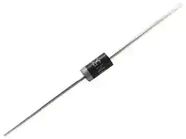


1N5338B-TP
ZENER DIODE, 5W, 5.1V, DO-15
- Manufacturer: MICRO COMMERCIAL COMPONENTS
- Product type: Zener Single Diodes
- No. of Pins: 2Pins
- Product Range: 1N53 Series
- Diode Case Style: DO-15
- Power Dissipation: 5W
- Zener Voltage Nom: 5.1V
- Operating Temperature Max: 150°C
| Delivery and price | |
|---|---|
| Units per pack | 1 |
| Price | 0.153 € |
| Current stock | 10+ |
| Lead time | 30 days |
## _M C C_

TM ������������������omponents 20736 Marilla Street Chatsworth �������� ��������������������� ���������������������

## **Micro Commercial Components**

## Features

- �� Zener Voltage From 5.1V to 51V

- Case Material: Molded Plastic. UL Flammability Classification Rating 94V-0

- �� For Available Tolerances—See Note 1

## **1N5338B THRU 1N5369B**

**5 Watt Zener Diode 5.1 to 51 Volts**

- Marking : Cathode band and type number

## Maximum Ratings:

- �� Operating Temperature: -55�C to +150�C

DO-15

- �� Storage Temperature: -55�C to +150�C

- �� 5 Watt DC Power Dissipation

- �� Maximum Forward Voltage @ 1A: 1.2 Volts

- �� Power Derating: 40 mW/� Above 75�

## Mechanical Characteristics

Case: JEDEC DO-15.

Terminals: Solder plated , solderable per MIL-STD-750, Method 2026.

Standard Packaging: 52mm tape

**==> picture [191 x 261] intentionally omitted <==**

**----- Start of picture text -----**<br>
D<br>A<br>Cathode<br>Mark<br>B<br>D<br>C<br>DIMENSIONS<br>INCHES MM<br>DIM MIN MAX MIN MAX NOTE<br>A .230 .300 5.80 7.60<br>B .104 .140 2.60 3.60<br>C .026 .034 .70 .90<br>D 1.000 --- 25.40 ---<br>**----- End of picture text -----**<br>


_www.mccsemi.com_

Revision: 4                                                                                                                         2006/06/09 **1 of 6**

## M C C

**==> picture [143 x 6] intentionally omitted <==**

**----- Start of picture text -----**<br>
TM<br>**----- End of picture text -----**<br>


## **1N5338B THRU 1N5369B**

**Micro Commercial Components**

ELECTRICAL CHARACTERISTICS (TA=25�C unless otherwise noted, VF=1.2 Max @ IF=1A for all types).

|MCC PART<br>NUMBER|REGULATOR<br>VOLTAGE<br>VZ|TEST<br>CURRENT<br>IZT|MAXIMUM<br>DYNAMIC<br>IMPEDANCE<br>ZZk<br>(@IZT)<br>(Note2)|MAXIMUM<br>REVERSE<br>CURRENT<br>IR|TEST<br>VOLTAGE<br>VR|MAXIMUM<br>REGULATOR<br>CURRENT<br>IZM|MAXIMUM<br>DYNAMIC<br>KNEE<br>IMPEDANCE<br>ZZK@ 1.0mA|MAXIMUM<br>SURGE<br>CURRENT<br>Ir|MAXIMUM<br>VOLTAGE<br>REGULATION<br>|
|---|---|---|---|---|---|---|---|---|---|
|||||||||||
||(Note2)|||||||||
|||||||(Note5)|(Note2)|(Note3)|(Note4)|
||VOLTS|mA|OHMS|�A|VOLTS|mA|ohms|A|VOLTS|
|1N5338B|5.1|240|1.5|1.0|1.0|930|400|14.4|0.39|
|1N5339B|5.6|220|1.0|1.0|2.0|865|400|13.4|0.25|
|1N5340B|6.0|200|1.0|1.0|3.0|790|300|12.7|0.19|
|1N5341B|6.2|200|1.0|1.0|3.0|765|200|12.4|0.10|
|1N5342B|6.8|175|1.0|10|5.2|700|200|11.5|0.15|
|1N5343B|7.5|175|1.5|10|5.7|630|200|10.7|0.15|
|1N5344B|8.2|150|1.5|10|6.2|580|200|10|0.20|
|1N5345B|8.7|150|2.0|10|6.6|545|200|9.5|0.20|
|1N5346B|9.1|150|2.0|7.5|6.9|520|150|9.2|0.22|
|1N5347B|10|125|2.0|5.0|7.6|475|125|8.6|0.22|
|1N5348B|11|125|2.5|5.0|8.4|430|125|8.0|0.25|
|1N5349B|12|100|2.5|2.0|9.1|395|125|7.5|0.25|
|1N5350B|13|100|2.5|1.0|9.9|365|100|7.0|0.25|
|1N5351B|14|100|2.5|1.0|10.6|340|75|6.7|0.25|
|1N5352B|15|75|2.5|1.0|11.5|315|75|6.3|0.25|
|1N5353B|16|75|2.5|1.0|12.2|295|75|6.0|0.30|
|1N5354B|17|70|2.5|0.5|12.9|280|75|5.8|0.35|
|1N5355B|18|65|2.5|0.5|13.7|264|75|5.5|0.40|
|1N5356B|19|65|3.0|0.5|14.4|250|75|5.3|.040|
|1N5357B|20|65|3.0|0.5|15.2|237|75|5.1|.040|
|1N5358B|22|50|3.5|0.5|16.7|216|75|4.7|0.45|
|1N5359B|24|50|3.5|0.5|18.2|198|100|4.4|0.55|
|1N5360B|25|50|4.0|0.5|19|190|110|4.3|0.55|
|1N5361B|27|50|5.0|0.5|20.6|176|120|4.1|0.60|
|1N5362B|28|50|6.0|0.5|21.2|170|130|3.9|0.60|
|1N5363B|30|40|8.0|0.5|22.8|158|140|3.7|0.60|
|1N5364B|33|40|10|0.5|25.1|144|150|3.5|0.60|
|1N5365B|36|30|11|0.5|27.4|132|160|3.3|0.65|
|1N5366B|39|30|14|0.5|29.7|122|170|3.1|0.65|
|1N5367B|43|30|20|0.5|32.7|110|190|2.8|0.70|
|1N5368B|47|25|25|0.5|35.8|100|210|2.7|0.80|
|1N5369B|51|25|27|0.5|38.8|93|230|2.5|0.90|


## NOTE:

1. TOLERANCE AND VOLTAGE DESIGNATION - The JEDEC type numbers shown indicate a tolerance of+/-10% with guaranteed limits on only Vz, IR, Ir, and VF as shown in the electrical characteristics table. Units with guaranteed limits on all seven parameters are indicated by suffix “B” for+/-5% tolerance.

2. ZENER VOLTAGE (Vz) AND IMPEDANCE (ZZT & ZZK) - Test conditions for Zener voltage and impedance are as follows; Iz is applied 40+/-10 ms prior to reading. Mounting contacts are located from the inside edge of mounting clips to the body of the diode(Ta=25    )�C

## _www.mccsemi.com_

Revision: 4                                                                                                                         2006/06/09 **2 of 6**

## _M C C_

**==> picture [145 x 6] intentionally omitted <==**

**----- Start of picture text -----**<br>
TM<br>**----- End of picture text -----**<br>


## **Micro Commercial Components**

## **1N5338B THRU 1N5369B**

3. SURGE CURRENT (Ir) - Surge current is specified as the maximum allowable peak, non-recurrent square-wave current with a pulse width, PW, of 8.3 ms. The data given in Figure 5 may be used to find the maximum surge current for a quare wave of any pulse width between 1 ms and 1000ms by plotting the applicable points on logarithmic paper. Examples of this, using the 6.8v and 200V zeners, are shown in Figure 6. Mounting contact located as specified in Note 3. (TA=25 � ).

4. VOLTAGE REGULATION (Vz) - Test conditions for voltage regulation are as follows: Vz measurements are made at 10% and then at 50% of the Iz max value listed in the electrical characteristics table. The test currents are the same for the 5% and 10% tolerance devices. The test current time druation for each Vz measurement is 40+/- 10 ms.

(TA=25C ). Mounting contact located as specified in Note2.

5. MAXIMUM REGULATOR CURRENT (IZM) - The maximum current shown is based on the maximum voltage of a 5% type unit. Therefore, it applies only to the B-suffix device. The actual IZM for any device may not exceed the value of 5 watts divided by the actual Vz of the device. TL=75Cat maximum from the device body.

## APPLICATION NOTE:

Since the actual voltage available from a given zener diode is temperature dependent, it is necessary to determine junction temperature under any set of operating conditions in order to calculate its value. The following procedure is recommended:

Lead Temperature, TL, should be determined from:

TL =th LAPD + TA

th LA is the lead-to-ambient thermal resistance ( /W) and PD is the power dissipation.

Junction Temperature, TJ , may be found from:

TJ = TL + TJL

TJL is the increase in junction temperature above the lead temperature and may be found from Figure 3 for a train of power pulses or from Figure 4 for dc power.

T JL = JL[P] D

For worst-case design, using expected limits of Iz, limits

of PD and the extremes of TJ(TJ) may be estimated. Changes in voltage, Vz, can then be found from:

, the zener voltage temperature coefficient, is fount from Figures 2.

Under high power-pulse operation, the zener voltage will vary with time and may also be affected significantly be the zener resistance. For best regulation, keep current excursions as low as possible.

Data of Figure 3 should not be used to compute surge capability. Surge limitations are given in Figure 5. They are lower than would be expected by considering only junction temperature, as current crowding effects cause temperatures to be extremely high in small spots resulting in device degradation should the limits of Figure. 5 be exceeded.

_www.mccsemi.com_

Revision: 4                                                                                                                         2006/06/09 **3 of 6**

e@ e _M C C_

TM

RATING AND CHARACTERISTICS CURVES 1N5338B THRU 1N5369B

## **Micro Commercial Components**

TEMPERATURE COEFFICIENTS

**==> picture [192 x 168] intentionally omitted <==**

**----- Start of picture text -----**<br>
es<br>r | [| | [| fe<br>rf; | [| [| | | |<br>i a<br>|<br>8 | of[| | tf| fffT[tt<br>L = LEAD LENGTH TO<br>6 Pf | HEAT SINK<br>(SEE FIGURE 5)<br>P<br>4 p of| fT| | w<br>a ee ee<br>2 rr h<br>ee<br>0 ee<br>0     20     40     60      80    100    120<br>TL, LEAD TEMPERATURE<br>PD, MAXIUMU POWER DISSIPATION (WATTS)<br>**----- End of picture text -----**<br>


**==> picture [208 x 118] intentionally omitted <==**

**----- Start of picture text -----**<br>
300200 FEREEEEEE<br>LT EEE REE EEE<br>100  { [| | Pte eeee<br>SSeS===Se0e>—-—, 2<br>RANGE<br>50<br>30 [TTTIAYwSeeera  se| cee FREESee<br>20<br>TT Tee tT et PT TTT TJ<br>10 HCOVA>. .=—=EEE SSS AA  =———==——————<br>5 |<br>0 a 20 40 ce 60 ce 80 100 120 140 160 180 200 220<br>VZ, ZENER VOLTAGE @IZT (VOLTS)<br>VZ, TEMPERATURE<br>COEFFICIENT (mA/_@IZT<br>**----- End of picture text -----**<br>


Fig. 1-POWER TEMPERATURE DERATING CURVE

Fig. 2-TEMPERATURE COEFFICIENT-RANGE FOR UNITS 6 TO 51 VOLTS

**==> picture [505 x 318] intentionally omitted <==**

**----- Start of picture text -----**<br>
30<br>20 D = 0.5 PTT Ty ET<br>I EE TE PE TT a<br>10 0.2 ee<br>O S ee TT eer<br>7 PS SS Sar tH<br>5 0.1 S e ae in<br>3 ESSPeeree er PPE f° tie rHCr<br>0.05<br>2 e iscortTrim rrr<br>0.02 NOTE BELOW 0.1 SECOND,<br>1 eee=::--— ——- THERMAL RESPONSE rs DUTY CYCLE, D = t1 / t2 rn<br>0.7 aa ee eee a0 CURVE IS APPLICABLE TO [oo: SINGLE PULSE TJL = JL(t)PPK 1<br>0.50.3 anSea.et 0.01 Si D = 0 eeeCTa ANY LEAD LENGTH (L) i!HH REPETITIVE PULSES TJL = JL(t,D)PPK<br>0.0001 0.0002 0.0005 0.001 0.002 0.005 0.01 0.02 0.05 0.1 0.2 0.5 1 2 5 10<br>TIME (SECONDS)<br>Fig. 3-TYPICAL THERMAL RESPONSE<br>40 Ft itt PW = 1ms* [TTT<br>20<br>40 TT eT ey yt yt peer te 10 SecseieeSassers, = eee a PW = 8.3ms*<br>30<br>4<br>20 FEC) 2 eas e PSL [><br>avama MOUNT ON 8.0mm2 1 EEESSSee PW = 1000ms* = SS Ss<br>10 COPPER PADS TO 0.4<br>0  0       0.2 rPo| 0.4       0.6EACH TERMINAL0.8       1 |aPt| |teft fteyft tt 0.20.1 SEFert = ACA SINE / SQUARE StTF WAVE PW aES = 100ms* FtSPS+}<br>3 4 6 8 10 20 30 40 60 80 100 200<br>L, LEAD LENGTH TO HEAT SINK (INCH) NOMINAL VZ(V)<br>LEAD(/W)<br>JL(t,D), TRANSIENT THERMAL RESISTANCE JUNCTION-TO-<br>/W)<br>C<br>RESISTANCE (<br>JL, JUNCTION-TO -LEAD THERMAL IR, PEAK SURGE CURRENT (AMPS)<br>**----- End of picture text -----**<br>


Fig. 4-TYPICAL THERMAL RESISTANCE

Fig. 5-MAXIMUM NON-REPETITIVE SURGE CURRENT VERSUS NOMINAL ZENER VOLTAGE (SEE NOTE 3)

## _www.mccsemi.com_

Revision: 4                                                                                                                         2006/06/09 **4 of 6**

## M C C

RATING AND CHARACTERISTICS CURVES 1N5338B THRU 1N5369B

**==> picture [143 x 6] intentionally omitted <==**

**----- Start of picture text -----**<br>
TM<br>**----- End of picture text -----**<br>


## **Micro Commercial Components**

ZENER VOLTAGE VERSUS ZENER CURRENT (FIGURES 7,8)

**==> picture [442 x 134] intentionally omitted <==**

**----- Start of picture text -----**<br>
30<br>20 VZ = 6.8V TC = 25 T = 25<br>10 1000<br>5<br>PLOTTED FROM INFORMATION<br>GIVEN IN FIGURE 6 100<br>2<br>1 10<br>0.5<br>1<br>0.2<br>0.1 0.1<br>1 10 100 1000 1 2 3 4 5 6 7 8 9 10<br>VZ, ZENER VOLTAGE (VOLTS)<br>IZ, ZENER CURRENT (mA)<br>**----- End of picture text -----**<br>


Fig. 6-PEAK SURGE CURRENT VERSUS PULSE WIDTH(SEE NOTE 3)

Fig. 7-ZENER VOLTAGE VERSUS ZENER CURRENT VZ = 6.8 THRU 10 VOLTS

**==> picture [234 x 151] intentionally omitted <==**

**----- Start of picture text -----**<br>
1000<br>T = 25<br>100<br>  10<br>   1<br>0.1<br>    10       20       30       40        50       60 [70       80]<br>VZ, ZENER VOLTAGE (VOLTS)<br>IZ, ZENER CURRENT (mA)<br>**----- End of picture text -----**<br>


Fig. 8-ZENER VOLTAGE VERSUS ZENER CURRENT VZ = 11 THRU 51 VOLTS

*** Data of Figure 3 should not be used to compute surge capability. Surge limitations are given in Figure 5. They are lower than would be expected by considering only junction temperature, as current crowding effects cause temperatures to be extremely high in small spots resulting in device degradation should the limits of Figure. 5 be exceeded

## www.mccsemi.com

Revision: 4                                                                                                                         2006/06/09 **5 of 6**

## M C C

**==> picture [144 x 7] intentionally omitted <==**

**----- Start of picture text -----**<br>
TM<br>**----- End of picture text -----**<br>


## **Micro Commercial Components**

## *****IMPORTANT NOTICE*****

_**Micro Commercial Components Corp .**_ reserves the right to make changes without further notice to any product herein to make corrections, modifications , enhancements , improvements , or other changes . _**Micro Commercial Components Corp .**_ does not assume any liability arising out of the application or use of any product described herein; neither does it convey any license under its patent rights ,nor the rights of others . The user of products in such applications shall assume all risks of such use and will agree to hold _**Micro Commercial Components Corp .**_ and all the companies whose products are represented on our website, harmless against all damages.

## *****APPLICATIONS DISCLAIMER*****

Products offer by _**Micro Commercial Components Corp .**_ are not intended for use in Medical, Aerospace or Military Applications.

## www.mccsemi.com

**6 of 6**

Revision: 4                                                                                                                         2006/06/09
Updated at February 9, 2023
Headquartered in the United States, Micro Commercial Components (MCC) is an established leader in the discrete semiconductor market. Leveraging vertical integration and an in-house wafer foundry, the company delivers high-quality, cost-effective components with competitive lead times. MCC's robust manufacturing capabilities allow them to support a wide array of demanding applications across the industrial, automotive, and consumer electronics sectors. The core of our MCC portfolio centers on a comprehensive selection of reliable diodes and rectifiers. This encompasses a strong variety of Zener single diodes designed for precise voltage regulation, alongside standard recovery, fast, and ultrafast rectifier diodes for efficient power management. Furthermore, MCC's small signal and Schottky diodes provide versatile, high-performance solutions for high-speed switching and applications requiring low forward voltage drops. Complementing their diode technologies, MCC manufactures a dependable lineup of bipolar transistors, as well as single and dual MOSFETs suited for diverse amplification and power switching tasks. By maintaining rigorous quality standards and a commitment to continuous process improvement, MCC remains a trusted partner for engineers seeking robust discrete semiconductors that enhance overall system reliability and performance.
About Novapart
Novapart is a B2B electronic component broker specialising in stock shortages and cost reduction. We source hard-to-find parts and identify compliant alternatives across a catalogue of 410,000+ components from 500+ manufacturers.
Learn more →Stock Shortage Specialist
When a component is unavailable, discontinued or has an unacceptable lead time, we tap into our network of vetted European and Asian distributors to source what you need — without compromising on quality or traceability.
Request a quote →Compliant Alternatives
We identify pin-to-pin, electrically equivalent substitutes that meet the same certifications (RoHS, AEC-Q100, REACH) as your original specification — validated against datasheets, not just part numbers. Often at a lower cost.
BOM Analysis service →