
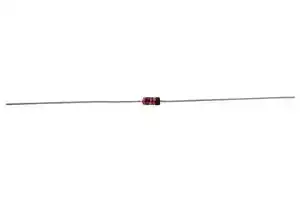


1N5250B
Zener Single Diode, 20 V, 500 mW, DO-35, 2 Pins, 200 °C, Through Hole
- Manufacturer: ONSEMI
- Product type: Zener Single Diodes
- Zener Voltage Vz Typ:20V; Power Dissipation Pd:500mW; Diode Case Style:DO-35; Zener Tolerance ±:5%; No. of Pins:2Pins; Operating Temperature Max:200°C; Product Range:1N52xxB Series; Autom
- SVHC: No SVHC (25-Jun-2025)
- No. of Pins: 2Pins
- Product Range: 1N52xxB
- Qualification: -
- Diode Mounting: Through Hole
- Diode Case Style: DO-35
- Power Dissipation: 500mW
- Zener Voltage Nom: 20V
- Operating Temperature Max: 200°C
| Delivery and price | |
|---|---|
| Units per pack | 5000 |
| Price | 0.01 € |
| Current stock | 10+ |
| Lead time | 30 days |
## **Is Now Part of**

## **To learn more about ON Semiconductor, please visit our website at www.onsemi.com**

Please note: As part of the Fairchild Semiconductor integration, some of the Fairchild orderable part numbers will need to change in order to meet ON Semiconductor’s system requirements. Since the ON Semiconductor product management systems do not have the ability to manage part nomenclature that utilizes an underscore (_), the underscore (_) in the Fairchild part numbers will be changed to a dash (-). This document may contain device numbers with an underscore (_). Please check the ON Semiconductor website to verify the updated device numbers. The most current and up-to-date ordering information can be found at www.onsemi.com. Please email any questions regarding the system integration to Fairchild_questions@onsemi.com.

ON Semiconductor and the ON Semiconductor logo are trademarks of Semiconductor Components Industries, LLC dba ON Semiconductor or its subsidiaries in the United States and/or other countries. ON Semiconductor owns the rights to a number of patents, trademarks, copyrights, trade secrets, and other intellectual property. A listing of ON Semiconductor’s product/patent coverage may be accessed at www.onsemi.com/site/pdf/Patent-Marking.pdf. ON Semiconductor reserves the right to make changes without further notice to any products herein. ON Semiconductor makes no warranty, representation or guarantee regarding the suitability of its products for any particular purpose, nor does ON Semiconductor assume any liability arising out of the application or use of any product or circuit, and specifically disclaims any and all liability, including without limitation special, consequential or incidental damages. Buyer is responsible for its products and applications using ON Semiconductor products, including compliance with all laws, regulations and safety requirements or standards, regardless of any support or applications information provided by ON Semiconductor. “Typical” parameters which may be provided in ON Semiconductor data sheets and/or specifications can and do vary in different applications and actual performance may vary over time. All operating parameters, including “Typicals” must be validated for each customer application by customer’s technical experts. ON Semiconductor does not convey any license under its patent rights nor the rights of others. ON Semiconductor products are not designed, intended, or authorized for use as a critical component in life support systems or any FDA Class 3 medical devices or medical devices with a same or similar classification in a foreign jurisdiction or any devices intended for implantation in the human body. Should Buyer purchase or use ON Semiconductor products for any such unintended or unauthorized application, Buyer shall indemnify and hold ON Semiconductor and its officers, employees, subsidiaries, affiliates, and distributors harmless against all claims, costs, damages, and expenses, and reasonable attorney fees arising out of, directly or indirectly, any claim of personal injury or death associated with such unintended or unauthorized use, even if such claim alleges that ON Semiconductor was negligent regarding the design or manufacture of the part. ON Semiconductor is an Equal Opportunity/Affirmative Action Employer. This literature is subject to all applicable copyright laws and is not for resale in any manner.

December 2018

## **1N5221B - 1N5263B Zener Diodes**

**==> picture [83 x 102] intentionally omitted <==**

**----- Start of picture text -----**<br>
Tolerance = 5%<br>DO-35 Glass case<br>COLOR BAND DENOTES CATHODE<br>**----- End of picture text -----**<br>


## **Absolute Maximum Ratings**

Stresses exceeding the absolute maximum ratings may damage the device. The device may not function or be operable above the recommended operating conditions and stressing the parts to these levels is not recommended. In addition, extended exposure to stresses above the recommended operating conditions may affect device reliability. The absolute maximum ratings are stress ratings only. Values are at TA = 25°C unless otherwise noted.

|**Symbol**|**Parameter**||**Value**|**Unit**|
|---|---|---|---|---|
|PD|Power Dissipation||500|mW|
||Derate above 50°C||4.0|mW°C|
|TSTG|Storage Temperature Range||-65 to +200|°C|
|TJ|Operating Junction Temperature Range||-65 to +200|°C|
||Lead Temperature (1/16 inch from case for 10 s)||+230|°C|


## **Note:**

1. These ratings are limiting values above which the serviceability of any semiconductor device may be impaired. Non-recurrent square wave Pulse Width = 8.3 ms, TA = 50°C

© 2018 Semiconductor Components Industries, LLC. 1N5221B - 1N5263B Rev. 3

www.onsemi.com

## **Electrical Characteristics**

° Values are at TA = 25 C unless otherwise noted .

|**Device**|**VZ (V) @ IZ **(2)|**VZ (V) @ IZ **(2)|**VZ (V) @ IZ **(2)|**ZZ (**Ω**) @ IZ (mA)**|**ZZ (**Ω**) @ IZ (mA)**|**ZZK (**Ω**) @ IZK(mA)**|**ZZK (**Ω**) @ IZK(mA)**|**IR (**μ**A) @ VR (V)**|**IR (**μ**A) @ VR (V)**|**TC**<br>**(%/**°**C)**|
|---|---|---|---|---|---|---|---|---|---|---|
||**Min.**|**Typ.**|**Max.**||||||||
|1N5221B|2.28|2.4|2.52|30|20|1,200|0.25|100|1.0|-0.085|
|1N5222B<br>1N5223B<br>1N5224B<br>1N5225B|2.375<br>2.565<br>2.66<br>2.85|2.5<br>2.7<br>2.8<br>3|2.625<br>2.835<br>2.94<br>3.15|30<br>30<br>30<br>29|20<br>20<br>20<br>20|1,250<br>1,300<br>1,400<br>1,600|0.25<br>0.25<br>0.25<br>0.25|100<br>75<br>75<br>50|1.0<br>1.0<br>1.0<br>1.0|-0.085<br>-0.080<br>-0.080<br>-0.075|
|1N5226B<br>1N5227B<br>1N5228B<br>1N5229B<br>1N5230B|3.135<br>3.42<br>3.705<br>4.085<br>4.465|3.3<br>3.6<br>3.9<br>4.3<br>4.7|3.465<br>3.78<br>4.095<br>4.515<br>4.935|28<br>24<br>23<br>22<br>19|20<br>20<br>20<br>20<br>20|1,600<br>1,700<br>1,900<br>2,000<br>1,900|0.25<br>0.25<br>0.25<br>0.25<br>0.25|25<br>15<br>10<br>5.0<br>5.0|1.0<br>1.0<br>1.0<br>1.0<br>2.0|-0.07<br>-0.065<br>-0.06<br>+/-0.055<br>+/-0.03|
|1N5231B<br>1N5232B<br>1N5233B<br>1N5234B<br>1N5235B|4.845<br>5.32<br>5.7<br>5.89<br>6.46|5.1<br>5.6<br>6<br>6.2<br>6.8|5.355<br>5.88<br>6.3<br>6.51<br>7.14|17<br>11<br>7.0<br>7.0<br>5.0|20<br>20<br>20<br>20<br>20|1,600<br>1,600<br>1,600<br>1,000<br>750|0.25<br>0.25<br>0.25<br>0.25<br>0.25|5.0<br>5.0<br>5.0<br>5.0<br>3.0|2.0<br>3.0<br>3.5<br>4.0<br>5.0|+/-0.03<br>0.038<br>0.038<br>0.045<br>0.05|
|1N5236B<br>1N5237B<br>1N5238B<br>1N5239B<br>1N5240B|7.125<br>7.79<br>8.265<br>8.645<br>9.5|7.5<br>8.2<br>8.7<br>9.1<br>10|7.875<br>8.61<br>9.135<br>9.555<br>10.5|6.0<br>8.0<br>8.0<br>10<br>17|20<br>20<br>20<br>20<br>20|500<br>500<br>600<br>600<br>600|0.25<br>0.25<br>0.25<br>0.25<br>0.25|3.0<br>3.0<br>3.0<br>3.0<br>3.0|6.0<br>6.5<br>6.5<br>7.0<br>8.0|0.058<br>0.062<br>0.065<br>0.068<br>0.075|
|1N5241B<br>1N5242B<br>1N5243B<br>1N5244B<br>1N5245B|10.45<br>11.4<br>12.35<br>13.3<br>14.25|11<br>12<br>13<br>14<br>15|11.55<br>12.6<br>13.65<br>14.7<br>15.75|22<br>30<br>13<br>15<br>16|20<br>20<br>9.5<br>9.0<br>8.5|600<br>600<br>600<br>600<br>600|0.25<br>0.25<br>0.25<br>0.25<br>0.25|2.0<br>1.0<br>0.5<br>0.1<br>0.1|8.4<br>9.1<br>9.9<br>10<br>11|0.076<br>0.077<br>0.079<br>0.080<br>0.082|
|1N5246B<br>1N5247B<br>1N5248B<br>1N5249B<br>1N5250B|15.2<br>16.15<br>17.1<br>18.05<br>19|16<br>17<br>18<br>19<br>20|16.8<br>17.85<br>18.9<br>19.95<br>21|17<br>19<br>21<br>23<br>25|7.8<br>7.4<br>7.0<br>6.6<br>6.2|600<br>600<br>600<br>600<br>600|0.25<br>0.25<br>0.25<br>0.25<br>0.25|0.1<br>0.1<br>0.1<br>0.1<br>0.1|12<br>13<br>14<br>14<br>15|0.083<br>0.084<br>0.085<br>0.085<br>0.086|
|1N5251B<br>1N5252B<br>1N5253B<br>1N5254B<br>1N5255B|20.9<br>22.8<br>23.75<br>25.65<br>26.6|22<br>24<br>25<br>27<br>28|23.1<br>25.2<br>26.25<br>28.35<br>29.4|29<br>33<br>35<br>41<br>44|5.6<br>5.2<br>5.0<br>4.6<br>4.5|600<br>600<br>600<br>600<br>600|0.25<br>0.25<br>0.25<br>0.25<br>0.25|0.1<br>0.1<br>0.1<br>0.1<br>0.1|17<br>18<br>19<br>21<br>21|0.087<br>0.088<br>0.088<br>0.089<br>0.090|
|1N5256B<br>1N5257B<br>1N5258B<br>1N5259B<br>1N5260B|28.5<br>31.35<br>34.2<br>37.05<br>40.85|30<br>33<br>36<br>39<br>43|31.5<br>34.65<br>37.8<br>40.95<br>45.15|49<br>58<br>70<br>80<br>93|4.2<br>3.8<br>3.4<br>3.2<br>3.0|600<br>700<br>700<br>800<br>900|0.25<br>0.25<br>0.25<br>0.25<br>0.25|0.1<br>0.1<br>0.1<br>0.1<br>0.1|23<br>25<br>27<br>30<br>33|0.09<br>0.092<br>0.093<br>0.094<br>0.095|
|1N5261B<br>1N5262B<br>1N5263B|44.65<br>48.45<br>53.2|47<br>51<br>56|49.35<br>53.55<br>58.8|105<br>125<br>150|2.7<br>2.5<br>2.2|1000<br>1100<br>1300|0.25<br>0.25<br>0.25|0.1<br>0.1<br>0.1|36<br>39<br>43|0.095<br>0.096<br>0.096|
||||||||||||
|**VF Forward**|**Voltage = 1.2V Max. @ IF = 200mA**||||||||||


## **Note:**

2. Zener Voltage (VZ) The zener voltage is measured with the device junction in the thermal equilibrium at the lead temperature (TL) at 30 ° C ± 1 ° C and 3/8” lead length.

© 2018 Semiconductor Components Industries, LLC. 1N5221B - 1N5263B Rev. 3

www.onsemi.com

2

## **Top Mark Information**

|**Device**|**Line 1**|**Line 2**|**Line 3**|
|---|---|---|---|
|1N5221B<br>1N5222B<br>1N5223B<br>1N5224B|LOGO<br>LOGO<br>LOGO<br>LOGO|22<br>22<br>22<br>22|1B<br>2B<br>3B<br>4B|
|1N5225B|LOGO|22|5B|
|1N5226B<br>1N5227B<br>1N5228B<br>1N5229B<br>1N5230B|LOGO<br>LOGO<br>LOGO<br>LOGO<br>LOGO|22<br>22<br>22<br>22<br>23|6B<br>7B<br>8B<br>9B<br>0B|
|1N5231B<br>1N5232B<br>1N5233B<br>1N5234B<br>1N5235B|LOGO<br>LOGO<br>LOGO<br>LOGO<br>LOGO|23<br>23<br>23<br>23<br>23|1B<br>2B<br>3B<br>4B<br>5B|
|1N5236B<br>1N5237B<br>1N5238B<br>1N5239B<br>1N5240B|LOGO<br>LOGO<br>LOGO<br>LOGO<br>LOGO|23<br>23<br>23<br>23<br>24|6B<br>7B<br>8B<br>9B<br>0B|
|1N5241B<br>1N5242B<br>1N5243B<br>1N5244B<br>1N5245B|LOGO<br>LOGO<br>LOGO<br>LOGO<br>LOGO|24<br>24<br>24<br>24<br>24|1B<br>2B<br>3B<br>4B<br>5B|
|1N5246B<br>1N5247B<br>1N5248B<br>1N5249B<br>1N5250B|LOGO<br>LOGO<br>LOGO<br>LOGO<br>LOGO|24<br>24<br>24<br>24<br>25|6B<br>7B<br>8B<br>9B<br>0B|
|1N5251B<br>1N5252B<br>1N5253B<br>1N5254B<br>1N5255B|LOGO<br>LOGO<br>LOGO<br>LOGO<br>LOGO|25<br>25<br>25<br>25<br>25|1B<br>2B<br>3B<br>4B<br>5B|
|1N5256B<br>1N5257B<br>1N5258B<br>1N5259B<br>1N5260B|LOGO<br>LOGO<br>LOGO<br>LOGO<br>LOGO|25<br>25<br>25<br>25<br>26|6B<br>7B<br>8B<br>9B<br>0B|
|1N5261B<br>1N5262B<br>1N5263B|LOGO<br>LOGO<br>LOGO|26<br>26<br>26|1B<br>2B<br>3B|
|||||


© 2018 Semiconductor Components Industries, LLC. 1N5221B - 1N5263B Rev. 3

www.onsemi.com

3

## **Top Mark Information** (Continued)

**22** le ~~ool~~ — **1B** ~~a=~~ **General Requirements:** 1.0 Cathode Band

1[st] line: ON Semiconductor Logo

2[nd] line: Device Name - 4[th] to 5[th] characters of the device name. or 5[th] to 6[th] characters for BZXyy series

3[rd] line: Device Name - 6[th] to 7[th] characters of the device name. or Voltage rating for BZXyy series

2.0 First Line: ON Semiconductor Logo

- 3.0 Second Line: Device name - For 1Nxx  series: 4[th] to 5[th] characters of the device name.

For BZxx series: 5[th] to 6[th] characters of the device name.

- 4.0 Third Line: Device name - For 1Nxx series: 6[th] to 7[th] characters of the device name.

For BZXyy series: Voltage rating

- 5.0 Devices shall be marked as required in the device specification (PID or ON Test Spec).

6.0 Maximum no. of marking lines: 3

- 7.0 Maximum no. of digits per line: 2

8.0 FSC logo must be 20 % taller than the alphanumeric marking and should occupy the 2 characters of the specified line.

9.0 Marking Font: Arial (Except ON Logo)

10.0 First character of each marking line must be aligned vertically.

11.0 All device markings must be based on ON Semiconductor device specification.

© 2018 Semiconductor Components Industries, LLC. 1N5221B - 1N5263B Rev. 3

www.onsemi.com

4

**==> picture [364 x 520] intentionally omitted <==**

**----- Start of picture text -----**<br>
T50 = 25.40 MIN (2X)<br>T26 = 14.00 MIN (2X)<br>[4.56]<br>3.05<br>0.533<br>NOTES: UNLESS OTHERWISE SPECIFIED<br>0.460<br>A) PACKAGE STANDARD REFERENCE:<br>JEDEC DO-204, VARIATION AH.<br>B) HERMETICALLY SEALED GLASS PACKAGE.<br>C) PACKAGE WEIGHT IS 0.137 GRAM.<br>D) ALL DIMENSIONS ARE IN MILLIMETERS.<br>E) DRAWING FILE NAME: DO35AREV03<br>**----- End of picture text -----**<br>


**==> picture [24 x 20] intentionally omitted <==**

**----- Start of picture text -----**<br>
1.91<br>1.53<br>**----- End of picture text -----**<br>


ON Semiconductor and      are trademarks of Semiconductor Components Industries, LLC dba ON Semiconductor or its subsidiaries in the United States and/or other countries. ON Semiconductor owns the rights to a number of patents, trademarks, copyrights, trade secrets, and other intellectual property. A listing of ON Semiconductor’s product/patent coverage may be accessed at www.onsemi.com/site/pdf/Patent−Marking.pdf. ON Semiconductor reserves the right to make changes without further notice to any products herein. ON Semiconductor makes no warranty, representation or guarantee regarding the suitability of its products for any particular purpose, nor does ON Semiconductor assume any liability arising out of the application or use of any product or circuit, and specifically disclaims any and all liability, including without limitation special, consequential or incidental damages. Buyer is responsible for its products and applications using ON Semiconductor products, including compliance with all laws, regulations and safety requirements or standards, regardless of any support or applications information provided by ON Semiconductor. “Typical” parameters which may be provided in ON Semiconductor data sheets and/or specifications can and do vary in different applications and actual performance may vary over time. All operating parameters, including “Typicals” must be validated for each customer application by customer’s technical experts. ON Semiconductor does not convey any license under its patent rights nor the rights of others. ON Semiconductor products are not designed, intended, or authorized for use as a critical component in life support systems or any FDA Class 3 medical devices or medical devices with a same or similar classification in a foreign jurisdiction or any devices intended for implantation in the human body. Should Buyer purchase or use ON Semiconductor products for any such unintended or unauthorized application, Buyer shall indemnify and hold ON Semiconductor and its officers, employees, subsidiaries, affiliates, and distributors harmless against all claims, costs, damages, and expenses, and reasonable attorney fees arising out of, directly or indirectly, any claim of personal injury or death associated with such unintended or unauthorized use, even if such claim alleges that ON Semiconductor was negligent regarding the design or manufacture of the part. ON Semiconductor is an Equal Opportunity/Affirmative Action Employer. This literature is subject to all applicable copyright laws and is not for resale in any manner.

## **PUBLICATION ORDERING INFORMATION**

**N. American Technical Support** : 800−282−9855 Toll Free USA/Canada

## **LITERATURE FULFILLMENT** :

Literature Distribution Center for ON Semiconductor

19521 E. 32nd Pkwy, Aurora, Colorado 80011 USA **Europe, Middle East and Africa Technical Support: Phone** : 303−675−2175 or 800−344−3860 Toll Free USA/Canada Phone: 421 33 790 2910 **Fax** : 303−675−2176 or 800−344−3867 Toll Free USA/Canada **Email** : orderlit@onsemi.com

**ON Semiconductor Website** : **www.onsemi.com**

**Order Literature** : http://www.onsemi.com/orderlit For additional information, please contact your local Sales Representative

© Semiconductor Components Industries, LLC

www.onsemi.com

**www.onsemi.com**

**1**
Updated at April 11, 2026
onsemi is a premier global supplier of intelligent power and sensing technologies, driving disruptive innovations across the automotive, industrial, and cloud infrastructure markets. Recognized for their commitment to sustainability and reliable supply chains, the company accelerates advancements in vehicle electrification, industrial automation, and 5G networks by solving the industry's most complex design challenges. At the core of their portfolio is an industry-leading selection of discrete semiconductors. This extensive range features thousands of high-performance bipolar transistors, single and dual MOSFETs, and a comprehensive array of diodes, including Zener, Schottky, and fast-recovery rectifiers. Engineered for superior thermal performance and energy efficiency, these foundational components are critical for demanding power conversion, switching, and signal conditioning applications. Beyond essential discretes, onsemi provides a robust suite of advanced power management and circuit protection solutions. Their lineup includes intelligent power modules, single IGBTs, and transient voltage suppression (TVS) diodes designed to safeguard sensitive circuitry. Complimented by integrated passive filters, AC/DC LED driver ICs, and specialized sub-2.4GHz RF transceivers, onsemi equips engineers with the scalable, high-quality technologies needed to build a cleaner, smarter, and more connected world.
About Novapart
Novapart is a B2B electronic component broker specialising in stock shortages and cost reduction. We source hard-to-find parts and identify compliant alternatives across a catalogue of 410,000+ components from 500+ manufacturers.
Learn more →Stock Shortage Specialist
When a component is unavailable, discontinued or has an unacceptable lead time, we tap into our network of vetted European and Asian distributors to source what you need — without compromising on quality or traceability.
Request a quote →Compliant Alternatives
We identify pin-to-pin, electrically equivalent substitutes that meet the same certifications (RoHS, AEC-Q100, REACH) as your original specification — validated against datasheets, not just part numbers. Often at a lower cost.
BOM Analysis service →