
Image not available
Illustrative purposes only

12151000
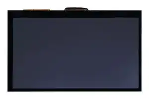
TFT LCD, 7 ", 1024 x 600 Pixels, Landscape, Black on White, 5V
⚠️ Reference pricing provided. In case of supply shortages, we will connect you with our trusted procurement partners to ensure your project's continuity.
- Manufacturer: TORADEX
- Product type: TFT LCD Displays
- SVHC: No SVHC (25-Jun-2025)
- VGA Size: -
- Resolution: 1024 x 600 Pixels
- Module Size: 164.9mm x 100mm
- Touchscreen: Projected Capacitive Touch
- Display Size: 7"
- Logic Voltage: 5V
- Product Range: -
- Display Pinout: 34 Way Connector
- Interface Type: MIPI DSI, I2C
- Display Appearance: Black on White
- Display Brightness: 800cd/m²
- Display Orientation: Landscape
- Operating Temperature Max: 70°C
- Operating Temperature Min: -20°C
| Delivery and price | |
|---|---|
| Units per pack | 1 |
| Price | 133.37 € |
| Current stock | 10+ |
| Lead time | 30 days |
Datasheet

# **Capacitive Touch Display 7" DSI** Datasheet

## TFT MODULE SPECIFICATION

## **RVT70HSDNWCA0**

HB, IPS 7.0” LCD TFT display datasheet Rev. 1.0 2024-12-10

## **Riverdi Sp. z o.o.**

Nowy Swiat 36 80-299 Gdansk, Poland VAT ID: PL5842767153 Registration number (KRS): 0000923967

**+48 587 703 116** Office hours: 9:00 to 17:30 CET (Mon-Fri) **contact@riverdi.com riverdi.com**

RVT70HSDNWCA0 iverd ITEM CONTENTS UNIT LCD Type TFT/Transmissive/Normally Black/IPS / Size 7.0 Inch Viewing Direction Free / ~~—~~ Outside Dimensions (W x H x D) 164.90 x 100.00 x 14.46 mm Active Area (W x H) 154.21 x 85.92 mm ~~eee~~ Pixel Pitch (W x H) 0.1506 x 0.1432 mm Resolution 1024 x 600 / ~~eee7~~ Brightness 800 cd/m[2] ~~a~~ Color Depth 16.7 M / ~~eeeoe~~ Pixel Arrangement RGB Vertical Stripe / ~~a~~ Driver IC of Board SN65DSI83 / ~~aeea~~ Interface MIPI DSI / ~~a~~ EEPROM Memory Size 2-Kbit / ~~aeea~~ Host Connector ZIF 34 pins, 0.5mm pitch, down-side contact / ~~a~~ With/Without Touch With Projected Capacitive Touch Panel / ~~a a~~ CTP Driver ILI2132A / ~~a~~ Supply Voltage for Module 5.0 V ~~a==a~~ Bonding Technology Air Bonding / ~~a~~ Weight 240 g ~~a=_~~ **Note 1.** RoHS3 compliant **Note 2.** LCM weight tolerance: ± 5%. © 2024 Riverdi Page 2 of 22 www.riverdi.com

© 2024 Riverdi

RVT70HSDNWCA0

## 1.

## **REVISION RECORD**

|REV NO.|REV DATE|CONTENTS|REMARKS|
|---|---|---|---|
|1.0|2024-12-10|Initial release||


© 2024 Riverdi

www.riverdi.com

Page 3 of 22

RVT70HSDNWCA0

## **CONTENTS**

|<br>2.|**CONTENTS**|
|---|---|
|1.|REVISION RECORD ............................................................................................................................................... 3|
|2.|CONTENTS .................................................................................................................................................................. 4|
|3.|MODULE CLASSIFICATION INFORMATION ............................................................................................. 5|
|4.|MODULE DRAWING ............................................................................................................................................... 6|
|5.|ABSOLUTE MAXIMUM RATINGS ..................................................................................................................... 7|
|6.|ELECTRICAL CHARACTERISTICS ................................................................................................................... 7|
|7.|BACKLIGHT ELECTRICAL CHARACTERISTICS ........................................................................................ 8|
|8.|ELECTRO-OPTICAL CHARACTERISTICS ..................................................................................................... 9|
|9.|INTERFACES DESCRIPTION ........................................................................................................................... 12|
||9.1<br>TFT OSSIQNMENTS......ssessssccssscsssccssccnsccssccssccsseccseceuscessccssecssccesecesscessccssecssccsssccusccssccssecsusccssecssecssecsscesssecssecsseeseesLZ|
|DIAGRAM BLOCK .......................................................................................................................................... 14<br>10.||
|TIMING CHARACTERISTICS ..................................................................................................................... 15<br>11,||
|CaPACITIVE TOUCH SCREEN PANEL SPECIFICATIONS ........................................................... 16<br>12.||
||V2.1<br>—Mechanical CHardcteristics ....ssssssssssssessssssssnssssssesssssssssesssseessssessssessssesssssssssesssscsssseesssessssssssssesssseesseeesseLO|
||12.2 — Electrical CHArACTEISTICS ......ssssssssssssescsssssssscssnscssssecsssecsssscsssscsssscsssscssssesssscsssseessscessssesssscsssssssssessssesssseesseLO|
|INSPECTION ..................................................................................................................................................... 17<br>13.||
||T3B.1<br>INSPECTION CONITION ......ecssessssscssccssscsseccssccssccssecsnscssecsssccssccssecsnecesscensccssccssecssccesccesscsssccsscsssccssecssscessccsseeseeLZ|
||TB.2<br>INSPECTION STANCAI.......sssssscsesssessesssscssccsecseccsssssscsscssscsscsusssssesscssccsscsuccascsuscssceuscssssuscssssasssucessssscesesssessesseeLO|
|RELIABILITY TEST ........................................................................................................................................ 20<br>14,||
|LEGAL INFORMATION ................................................................................................................................. 21<br>15.||
|16.|CONTACT .............................................................................................................................................................22<br>16.|


© 2024 Riverdi

www.riverdi.com

Page 4 of 22

RVT70HSDNWCA0

|**MODULE CLASSIFICATION INFORMATION**<br>RV<br>T<br>70<br>H<br>S<br>D<br>N<br>W<br>C<br>A0<br>V1.0A<br>1.<br>2.<br>3.<br>4.<br>5.<br>6.<br>7.<br>8.<br>9.<br>10.<br>11.<br>ee<br>e*<br>3.<br>~~ee.~~|
|---|


|NO.|PARAMETER|SYMBOL|
|---|---|---|
|1.|BRAND|RV – Riverdi|
|2.|PRODUCT TYPE|T – TFT Standard|
|3.|DISPLAY SIZE|70 – 7.0”|
|4.|MODEL SERIAL NO.|H – High Brightness, IPS|
|5.|RESOLUTION|S – 1024 x 600 px|
|6.|INTERFACE|D – MIPI DSI|
|7.|FRAME|N – Without Mounting Metal Frame|
|8.|BACKLIGHT TYPE|W – LED White|
|9.|TOUCH PANEL|C – With Capacitive Touch Panel|
|10.|PCAP VERSION|A0 – aTouch, Air Bonding|
|11.|MODULEVERSION|V1.0A|


© 2024 Riverdi

www.riverdi.com

Page 5 of 22

**==> picture [591 x 418] intentionally omitted <==**

**----- Start of picture text -----**<br>
Revision: Changes: Date:<br>1.0 Initial Case 2024.11.27<br>164.90 [6.492](TFT O.D.)<br>164.70 [6.484](CG O.D.) 0.10 [0.004]<br>163.66 [6.443](SENSOR O.D.) 0.94 [0.037] MAX 14.46 [0.569](MODULE O.D.)<br>156.08 [6.145](SENSOR A.A.) 6.14 [0.242] 8.15 [0.321](CTP+TFT)<br>155.01 [6.103](CG V.A.) 6.68 [0.263] 2.45 [0.096](CG+SCA+SENSOR+DST)<br>154.21 [6.071](TFT A.A.) 7.07 [0.278] 1.10 [0.043](CG) 63.25±0.5 [2.490±0.020]<br>80.72 [3.178] 13.49±0.5 [0.531±0.020]<br>A<br>(T=1.1mm[0.043inch])LENS 34 1 J1<br>SCA<br>(T=0.2mm[0.008inch]) 10 1<br>SENSOR<br>(T=0.55mm[0.022inch]) 4 0 1<br>DST<br>(T=0.6mm[0.024inch])<br>GROUNDING TAPE<br>BLACK MASK PRINTING<br>DETAIL A<br>RAL9005 SCALE 4:1 LEDA<br>0.20 [0.008]*45°<br>0.20 [0.008]*45°<br>LEDK<br>LED Diagram Circuit<br>PINOUT ON THE 2ND PAGE<br>TFT NOTES: TP NOTES: GENERAL NOTES:<br>1. LCD TYPE: TRANSMISSIVE, NORMALLY BLACK, IPS 1.  TP STRUCTURE: G+G 1. MODULE SURFACE LUMINANCE: 800 cd/m^2<br>2. RESOLUTION: 1024x600 2.  CG THICKNESS: 1.1mm[0.043inch] 2. AIR BONDING PN: RVT70HSDNWCA0<br>3.4. DRIVING IC ON THE BOARD: SN65DSI83ZXHRVIEWING ANGLE: FREE 3.4. DRIVER IC: ILI2132ASURFACE HARDNESS: 7H 3.4. OPERATING TEMPERATURE: -20°C ~ 70°CSTORAGE TEMPERATURE: -30°C ~ 80°C SN:<br>5.  INTERFACE: MIPI DSI6.  OPERATION VOLTAGE: 5.0V 5.  INTERFACE: I2C 5. ±0.3mm[0.012inch]WITHOUT INDIVIDUAL TOLERANCE:  DRAWN: M.Natywa 2024.11.27 1:1.39<br>6. RoHS3 COMPLIANT CHECKED: Carol Gao 2024.11.27 [mm]<br>APPR: ISO A3 P. 1 of 1<br>4*R0.30 [R0.012]<br>47.93 [1.887]<br>100.00 [3.937](TFT O.D.) 99.80 [3.929](CG O.D.) 98.55 [3.880](SENSOR O.D.) 88.42 [3.481](SENSOR A.A.) 86.72 [3.414](CG V.A.) 85.92 [3.383](TFT A.A)<br>0.10 [0.004] 0.63 [0.025] 3.72 [0.146] 4.57 [0.180] 4.97 [0.195]<br>24.10±0.5 [0.949±0.020] 20.00±0.5 [0.787±0.020]<br>CN1<br>4 1<br>**----- End of picture text -----**<br>


RVT70HSDNWCA0

## **ABSOLUTE MAXIMUM RATINGS**

|PARAMETER|SYMBOL|MIN|MAX|UNIT|
|---|---|---|---|---|
|Supply Voltage for Module|VDD|0|7.4|V|
|Reference Voltage|VREF|0|4.6|V|
|PWM Input Voltage|VPWM|-0.3|7.4|V|
|Operating Temperature|TOP|-20|70|°C|
|Storage Temperature|TST|-30|80|°C|
|Storage Humidity (@ 25 ± 5°C)|HST|10|-|% RH|
|Operating Ambient Humidity (@ 25 ±<br>5°C)|HOP|10|-|% RH|


**Note.** The above are maximum values. If exceeded, they may cause permanent damage to the unit.

## **ELECTRICAL CHARACTERISTICS**

|PARAMETER|SYMBOL|MIN|TYP|MAX|UNIT|NOTE|
|---|---|---|---|---|---|---|
|Supply Voltage for Module<br>~~eee~~|VDD<br>~~eee~~|-<br>~~eee~~|5.0<br>~~eee~~<br>~~7~~|-<br>~~eee~~|V<br>~~eee~~|~~eee~~|
|Reference Voltage<br>~~i~~<br>~~ee~~|VREF|0<br>~~ee~~|-<br>~~ee~~<br>~~Sy~~|3.6<br>~~ee~~<br>~~Sy~~|V<br>~~|~~<br>~~ee~~|Note 1<br>~~|~~<br>~~ee~~|
|Current drawn from VREF<br>~~ee~~<br>~~ee~~|IVREF<br>~~ee~~<br>~~a~~|-<br>~~ee~~<br>~~ee~~|1<br>~~ee~~<br>~~ee~~<br>~~Sy~~|-<br>~~ee~~<br>~~ee~~<br>~~Sy~~|uA<br>~~ee~~<br>~~ee~~|VREF=1.8V<br>~~ee~~<br>~~ee~~<br>~~ee~~|
|Input High Voltage<br>~~ee~~<br>~~ee~~|VIH<br>~~ee~~<br>~~==.~~|0.7VREF<br>~~ee ~~<br>~~ee~~<br>~~==.~~|-<br> ~~ee~~<br>~~ee~~<br>~~==.~~|-<br>~~ee~~<br>~~ee~~|V<br>~~ee~~<br>~~ee~~|~~ee~~<br>~~ee~~<br>~~ee~~<br>~~oe~~|
|Input Low Voltage<br>~~ee ~~<br>~~ee~~|VIL<br> ~~ee~~<br>~~==.~~|0<br>~~ee ~~<br>~~==.~~|-<br> ~~ee~~<br>~~==.~~|0.3VREF<br>~~ee~~<br>~~P|~~|V<br>~~ee~~<br>~~P|~~<br>~~|~~|~~ee~~<br>~~ee~~<br>~~oe~~|
|PWM Logic Input High<br>Voltage<br>~~ee~~<br>~~fe~~|VPWMH<br>~~fe~~<br>~~==.~~<br>~~—_~~|1.2<br>~~fe~~<br>~~==.~~|-<br>~~==.~~<br>~~:~~|VDD<br>~~P|~~<br>~~:~~|V<br>~~P|~~<br>~~|~~|Note 2<br>~~oe~~<br>~~oe~~|
|PWM Logic Input Low<br>Voltage<br>~~ee~~<br>~~fe~~<br>~~ee~~|VPWML<br>~~fe~~<br>~~—_~~|0<br>~~fe~~<br>~~=~~|-<br>~~=~~<br>~~{|~~|0.4<br>~~P|~~<br>~~{|~~<br>~~Pf~~|V<br>~~P|~~<br>~~|~~<br>~~{|~~<br>~~Pf~~<br>~~Oo~~|Note 2<br>~~oe~~<br>~~Oo~~|
|PWM Frequency<br>~~fe~~<br>~~ee~~|FPWM<br>~~fe~~<br>~~—_~~|200<br>~~fe~~<br>~~=~~|-<br>~~=~~<br>~~{|~~|200k<br>~~{|~~<br>~~Pf~~|Hz<br>~~{|~~<br>~~Pf~~<br>~~Oo~~|Note 3<br>~~oe~~<br>~~Oo~~|


© 2024 Riverdi

www.riverdi.com

Page 7 of 22

RVT70HSDNWCA0

**Note 1.** TYP of reference Voltage is 1.8V or 3.3V which is dependent on the SBC.

**Note 2.** PWM input is independent of VREF. Min of logic high level is 1.2V and max of logic low level is 0.4V.

**Note 3.** The backlight driver is DIO5661 and the recommended PWM frequency is 10kHz.

|PARAMETER|SYMBOL|BL 0%|BL 58 %|BL 100%|UNIT|NOTE|
|---|---|---|---|---|---|---|
|Current drawn from<br>VDD@5.0V|IVDD|194|450|737|mA|Note 3|


## **Note 3.**

BL 0%, current was measured with BL brightness set to 0%, BL 58%, current was measured with BL brightness set to 58%, BL 100%, current was measured with BL brightness set to 100%.

Test condition: ambient temperature 25[o] C, PCAP is in active mode. The IVDD current measurement was conducted based on Dahlia Carrier board + Verdin iMX8M. Backlight levels on Verdin iMX8M can be set from 0 to 7(8 levels).

|BACKLIGHT LEVEL|0%|**14.5%**|**29%**|**43.5%**|**58%**|**72.5%**|**85.5%**|**100%**|
|---|---|---|---|---|---|---|---|---|
|SOM BL SET|0|1|2|3|4|5|6|7|


## **BACKLIGHT ELECTRICAL CHARACTERISTICS**

|PARAMETER|SYMBOL|MIN|TYP|MAX|UNIT|NOTE|
|---|---|---|---|---|---|---|
|Lifetime|-|-|50,000|-|hours|Note 1|


**Note 1.** Unless specified, the ambient temperature Ta = 25℃

**Note 2.** The recommended operating conditions refer to a range in which operation of this product is guaranteed. The operation cannot be guaranteed if the absolute maximum values exceed.

**Note 3.** If LED is driven by high current, high ambient temperature and humidity condition, the lifetime of LED will be reduced. Operating life means brightness goes down to 50% initial brightness. Typical operating lifetime is estimated data.

© 2024 Riverdi

www.riverdi.com

Page 8 of 22

RVT70HSDNWCA0

## **ELECTRO-OPTICAL CHARACTERISTICS**

|ITEM|SYMBOL|CONDITION|MIN|TYP|MAX|UNIT|RMK|NOTE|
|---|---|---|---|---|---|---|---|---|
|Response Time<br>~~|~~<br>~~oe~~|Tr+Tf<br>~~|~~<br>~~oe~~|θ=0°<br>∅=0°<br>Ta=25 °C|-<br>~~Te~~|25<br>~~a~~<br>~~Te~~|35<br>~~PEt~~|ms<br>~~PEt~~|FIG 1.<br>~~PEt~~|4, 7<br>~~—~~<br>~~a~~|
|Contrast Ratio<br>~~oe~~|Cr<br>~~oe~~<br>~~ee~~||800<br>~~Te~~|1000<br>~~a~~<br>~~Te~~|-<br>~~PEt~~|---<br>~~PEt~~|FIG 2.<br>~~PEt~~|1, 7<br>~~a~~|
|Surface<br>Luminance<br>~~oe~~<br>~~oe~~|Lv<br>~~oe~~<br>~~—~~||-|800<br>~~a~~<br>~~_~~|-|cd/m<br>2||2, 7<br>~~a~~<br>~~_~~|
|Viewing Angle<br>Range<br>~~oe~~|θ<br>~~—~~<br>~~a~~<br>~~ia~~|∅ = 90°<br>|75<br>~~-~~<br>~~re~~|85<br>~~_~~<br>~~re~~|-<br>~~re~~|deg<br>~~re~~|FIG 3.|6<br>~~_~~|
|||∅ = 270°<br>|75<br>~~re~~<br>|85<br>~~re~~<br>|-<br>~~re~~<br>~~a~~|deg<br>~~re~~<br>~~a~~|||
|||∅ = 0°<br><br>|75<br>~~re~~<br> <br>~~in~~|85<br>~~re~~<br> <br>~~in~~|-<br>~~re~~<br> ~~a~~<br>~~in~~|deg<br>~~re~~<br>~~a~~<br>~~in~~|||
|||∅ = 180°<br><br>|75<br>~~re~~<br> <br>~~in~~|85<br>~~re~~<br> <br>~~in~~|-<br>~~re~~<br> <br>~~in~~|deg<br>~~re~~<br><br>~~in~~|||
|CIE (x, y)<br>Chromaticity|Rx<br>~~a~~<br>~~ia~~<br>~~ia~~|θ=0°<br>∅=0°<br>Ta=25 °C<br> <br> <br> <br>|0.578<br>~~re~~<br>~~- ~~<br>~~in~~<br>~~i~~|0.618<br>~~re~~<br> <br>~~in~~<br>~~i~~|0.658<br>~~re~~<br> <br>~~in~~<br>~~i~~|-<br>~~re~~<br><br>~~in~~<br>~~i~~|FIG 2.|5,7|
||Ry<br>~~a~~<br>~~ia~~<br>~~ia~~<br>~~a~~||0.489<br>~~re~~<br>~~in~~<br>~~i~~<br>~~=~~|0.329<br>~~re~~<br>~~in~~<br>~~i~~<br>~~=~~|0.369<br>~~re~~<br>~~in~~<br>~~i~~<br>~~=~~|-<br>~~re~~<br>~~in~~<br>~~i~~<br>~~=~~|||
||Gx<br>~~a ~~<br>~~ia~~<br>~~ia~~<br>~~a~~||0.376<br> ~~re~~<br>~~in~~<br>~~i~~<br>~~=~~<br>|0.416<br>~~re~~<br>~~in~~<br>~~i~~<br>~~=~~<br>|0.456<br>~~re~~<br>~~in~~<br>~~i~~<br>~~=~~<br>~~=~~|-<br>~~re~~<br>~~in~~<br>~~i~~<br>~~=~~<br>~~=~~|||
||Gy<br>~~ia~~<br>~~ia~~<br>~~a~~||0.493<br>~~in~~<br>~~i~~<br>~~=~~<br>|0.533<br>~~in~~<br>~~i~~<br>~~=~~<br>|0.573<br>~~in~~<br>~~i~~<br>~~=~~<br> ~~=~~<br>~~a~~|-<br>~~in~~<br>~~i~~<br>~~=~~<br>~~=~~<br>~~a~~|||
||Bx<br>~~ia ~~<br>~~ia~~<br>~~a~~||0.071<br> ~~in~~<br>~~i~~<br>~~=~~<br>|0.111<br>~~in~~<br>~~i~~<br>~~=~~<br>|0.151<br>~~in~~<br>~~i~~<br>~~=~~<br> <br>~~a~~<br>~~——~~|-<br>~~in~~<br>~~i~~<br>~~=~~<br><br>~~a~~<br>~~——~~|||
||By<br>~~ia~~<br>~~a~~||0.108<br>~~i~~<br>~~=~~<br>~~- ~~|0.148<br>~~i~~<br>~~=~~<br> <br>~~—~~|0.188<br>~~i~~<br>~~=~~<br> <br>~~——~~<br>~~—~~|-<br>~~i~~<br>~~=~~<br><br>~~——~~<br>~~—~~|||
||Wx<br>~~ia ~~<br>~~a ~~||0.270<br> ~~i~~<br> ~~=~~|0.310<br>~~i~~<br>~~=~~<br>~~—~~|0.350<br>~~i~~<br>~~=~~<br>~~—~~|-<br>~~i~~<br>~~=~~<br>~~—~~|||
||Wy<br>~~a~~||0.290|0.330<br>~~—~~|0.370<br>~~—~~|-<br>~~—~~|||


Lv = Average Surface Luminance with all white pixels (P1, P2, P3, P4, P5)

**Note 3.** The uniformity in surface luminance δ WHITE is determined by measuring luminance at each test position 1 through 5, and then dividing the minimum luminance of 5 points luminance by maximum luminance of 5 points luminance. For more information see Figure 2.

© 2024 Riverdi

www.riverdi.com

Page 9 of 22

RVT70HSDNWCA0

δ WHITE =[Minimum Surface Luminance with all white pixels (P1, P2, P3, P4, P5)] Maximum Surface Luminance with all white pixels (P1, P2, P3, P4, P5)

**Note 4.** Response time is the time required for the display to transition from white to black (Rise Time, Tr) and from black to white (Decay Time, Tf). For additional information see Figure 1. The test equipment is BM-7A.

**Note 5.** CIE (x, y) chromaticity, the x, y value is determined by measuring luminance at each test position 1 through 5, and then make average value.

**Note 6.** For TFT module, viewing angle is the angle at which the contrast ratio is greater 10. The angles are determined for the horizontal or x axis and the vertical or y axis with respect to the z axis which is normal to LCD surface. For more information see Figure 3.

**Note 7.** Viewing angle is measured at the center point of the LCD by CONOSCOPE (ergo-80). For response time testing, the testing data is based on BM-7A. Instruments for Contrast Ratio, Surface Luminance, Luminance Uniformity, Chromaticity the test data is based on SR3A.

Figure 1. The definition of response time

© 2024 Riverdi

www.riverdi.com

Page 10 of 22

RVT70HSDNWCA0

**==> picture [216 x 141] intentionally omitted <==**

**----- Start of picture text -----**<br>
_—lW Kr oemx ><br>Padi ‘A<br>faa} 1<br>[a] en<br>| [|] Wg :<br>**----- End of picture text -----**<br>


A: 5mm

B: 5mm

H, V: Active Area

Light spot size ∅=5mm, 500mm distance from the LCD surface to detector lens. Measurement instrument is SR-3A

Figure 2. Measuring method for Contrast ratio, surface luminance, Luminance uniformity, CIE (x, y) chromaticity

Figure 3. The definition of viewing angle

© 2024 Riverdi

www.riverdi.com

Page 11 of 22

RVT70HSDNWCA0

## **INTERFACES DESCRIPTION**

## **TFT assignment**

|PIN<br>~~ee~~|SYMBOL<br>~~ee~~|I/O<br>~~ee~~|DESCRIPTION<br>~~ee~~|NOTE<br>~~ee~~|
|---|---|---|---|---|
|**1**<br>~~ee~~|GND<br>~~ee~~|P<br>~~ee~~|Ground<br>~~ee~~|~~ee~~|
|**2**<br>~~ee ~~|DSI_D0P<br> ~~ee ~~<br>~~—~~|I/O<br> ~~ee~~<br>~~—~~|MIPI DSI differential data pair. (Data lane 0)<br>~~ee~~<br>~~oe~~<br>~~Be~~|~~ee ~~<br>~~oe~~|
|**3**<br>~~oe~~|DSI_D0N<br>~~—~~<br>~~oe~~|I/O<br>~~—~~<br>~~oe~~<br>~~Be~~||~~oe~~<br>~~=~~|
|**4**<br>~~oe~~<br>~~oo~~|GND<br>~~oe~~<br>~~oo~~|P<br>~~oe~~<br>~~Be~~<br>~~oo~~|Ground<br>~~Be~~<br>~~oo~~|~~=~~<br>~~oo~~|
|**5**<br>~~oo~~|DSI_D1P<br>~~oo~~|I<br>~~Be~~<br>~~oo~~|MIPI DSI differential data pair. (Data lane 1)<br>~~Be~~<br>~~oo~~|~~oo~~|
|**6**<br>~~oo~~<br>~~fF~~|DSI_D1N<br>~~oo~~<br>~~fF~~|I<br>~~oo~~<br>~~fF~~||~~oo~~<br>~~a~~|
|**7**<br>~~fF~~<br>~~ff~~|GND<br>~~fF~~<br>~~ff~~|P<br>~~fF~~<br>~~ff~~|Ground<br>~~ff~~|~~a~~<br>~~ff~~|
|**8**<br>~~|~~|DSI_CLKP<br>~~=.~~|I<br>~~=.~~|MIPI DSI differential clock pair<br>~~=.~~<br>~~ee~~|~~=.~~|
|**9**<br>~~|~~|DSI_CLKN<br>~~=.~~<br>~~a~~|I<br>~~=.~~<br>~~ee~~||~~=.~~<br>~~|~~<br>~~ee~~|
|**10**|GND<br>~~a~~|P<br>~~ee~~|Ground<br>~~ee~~|~~|~~<br>~~ee~~|
|**11**<br>~~a~~|DSI_D2P<br>~~a~~<br>~~a~~|I<br>~~ee~~<br>~~a~~|MIPI DSI differential data pair. (Data lane 2)<br>~~ee~~<br>~~:~~|~~ee~~<br>~~:~~|
|**12**<br>~~a~~<br>~~fF~~|DSI_D2N<br>~~a~~<br>~~fF~~|I<br>~~a~~<br>~~fF~~||~~:~~<br>~~M~~|
|**13**<br>~~fF~~<br>~~De~~|GND<br>~~fF~~<br>~~De~~|P<br>~~fF~~|Ground|~~M~~|
|**14**<br>~~De~~<br>~~==~~|DSI_D3P<br>~~De~~<br>~~==~~|I<br>~~==~~|MIPI DSI differential data pair. (Data lane 3)<br>~~=~~|~~=~~|
|**15**<br>~~==~~<br>~~ff~~|DSI_D3N<br>~~==~~<br>~~ff~~|I<br>~~==~~<br>~~ff~~||~~=~~<br>~~8~~|
|**16**<br>~~ff~~|GND<br>~~ff~~<br>~~a ~~|P<br>~~ff~~<br> ~~a ee~~|Ground<br>~~ee~~|~~8~~<br>~~ee~~|
|**17**<br>~~ees~~|PWR_DN<br>~~ees~~<br>~~ee~~|I<br>~~ees~~<br>~~ee~~|Power down (With locally generated reset<br>after releasing power-down)<br>Active Low, display is off when signal is low;<br>~~ees~~<br>~~ee~~|Note 2<br>~~ees~~|
|**18**|PWM<br>~~ee~~|I<br>~~ee~~|Backlight brightness control<br>~~ee~~|Note 3|
|**19**<br>~~mn~~|INT<br>~~ee~~<br>~~mn~~|O<br>~~ee~~<br>~~mn~~|Touch panel Interrupt signal;<br>Open-drain output, active low<br>~~ee~~<br>~~mn~~|Note 2<br>~~mn~~|


© 2024 Riverdi

www.riverdi.com

Page 12 of 22

RVT70HSDNWCA0

|**20**<br>~~|~~|I2C_SCL<br>|I<br>~~po~~|I2C clock signal<br>~~po~~|Note 2<br>~~po~~|
|---|---|---|---|---|
|**21**<br>~~| ~~|I2C_SDA<br> <br>~~ee~~|I/O<br> ~~po~~|I2C data signal<br>~~po~~||
|**22**|RESET|I|Touch panel reset||
|**23**<br>~~ee~~|NC<br>~~ee~~|/<br>~~ee~~|No connection<br>~~eee~~|~~eee~~|
|**24**<br>~~ee~~<br>~~=~~|VREF<br>~~ee~~<br>~~tf=~~|P<br>~~ee~~<br>~~tf~~|Reference voltage<br>~~eee~~<br>~~ee~~|~~eee~~|
|**25**<br>~~ee~~<br>~~{|~~<br>~~=~~|NC<br>~~ee~~<br>~~{|~~<br>~~tf=~~|/<br>~~ee ~~<br>~~{|~~<br>~~tf~~|No connection<br> ~~eee~~<br>~~ee~~|~~eee~~<br>~~a~~|
|**26**<br>~~=~~|5.0V<br>~~tf= ~~<br>~~ee~~|P<br>~~tf ~~<br>~~ee~~<br>~~7~~|Power supply VDD<br> ~~ee~~<br>~~ee~~|~~ee~~|
|**27**<br>~~=~~|||||
|**28**<br>~~=~~|||||
|**29**<br>~~=~~<br>~~ee~~|||||
|**30**<br>~~ee~~|GND<br>~~ee~~|P<br>~~ee~~|Ground<br>~~ee~~|~~ee~~<br>~~|~~<br>~~7~~|
|**31**<br>~~ee~~|NC<br>~~ee~~|/<br>~~ee~~|No connection<br>~~ee~~|~~ee~~<br>~~7~~|
|**32**|||||
|**33**|||||
|**34**<br>~~|~~|||||


**Note 1** . Matched 34 pins, 0.5 mm pitch, 150 mm long FFC accessory: FFC0534150

**Note 2.** Internally pull-up with 15K resistors to VREF   for pins 17, 19

Internally pull-up with 10K resistors to VREF  for pins 20, 21

**Note 3.** The backlight driver is DIO5661. PWM frequency range: 200Hz – 200KHz and the recommended PWM frequency is 10kHz.

0% PWM duty cycle corresponds to minimum brightness.

100 PWM duty cycle corresponds to maximum brightness.

© 2024 Riverdi

www.riverdi.com

Page 13 of 22

RVT70HSDNWCA0

## **DIAGRAM BLOCK**

© 2024 Riverdi

www.riverdi.com

Page 14 of 22

RVT70HSDNWCA0

## 11.

## **TIMING CHARACTERISTICS**

The TFT of the module applies Riverdi high brightness, IPS, 7.0” TFT: RVT70HSLNWCA0 For detailed information of the display, please refer to the datasheet of display.

|PARAMETER|SYMBOL|VALUE|VALUE|VALUE|UNIT|
|---|---|---|---|---|---|
|||MIN.|TYP.|MAX.||
|DCLK frequency<br>(Frame rate 60Hz)|Fclk|40.8|51.2|67.2|MHz|
|Horizontal display<br>area|Thd|1024|||DCLK|
|HSYNC period time|Th|1114|1344|1400||
|HSYNC blanking|Thb+Thfp|90|320|376||
|Vertical display area|Tvd|600|||H|
|VSYNC period time|Tv|610|635|800||
|VSYNC blanking|Tvb+Tvfp|10|85|200||


© 2024 Riverdi

www.riverdi.com

Page 15 of 22

RVT70HSDNWCA0

## **CAPACITIVE TOUCH SCREEN PANEL** 12. **SPECIFICATIONS**

## **Mechanical characteristics**

|DESCRIPTION|SPECIFICATION|REMARK|
|---|---|---|
|**Touch Panel Size**|7.0 inch|aTouch|
|**Outline Dimension of CTP**|164.70 mm x 99.80 mm||
|**Product Thickness**|2.45 mm||
|**Glass Thickness**|1.1 mm||
|**CTP View Area**|155.01 mm x 86.72 mm||
|**Sensor Active Area**|156.08 mm x 88.42 mm||
|**Surface Hardness**|7H||


## **Electrical characteristics**

|DESCRIPTION|SPECIFICATION|REMARK|
|---|---|---|
|**Linearity**|+/-1.5mm||
|**Controller**|ILI2132A||
|**Resolution**|1024 x 600||


© 2024 Riverdi

www.riverdi.com

Page 16 of 22

RVT70HSDNWCA0

## **INSPECTION**

Standard acceptance/rejection criteria for TFT module

## **Inspection condition**

Ambient conditions:

- Temperature: 25 ± 2°C

- Humidity: (60 ± 10) %RH

- Illumination: Single fluorescent lamp non-directive (300 to 700 lux)

Viewing distance: 35 ± 5cm between inspector bare eye and LCD.

Viewing Angle: U/D: 45°/45°, L/R: 45°/45°

© 2024 Riverdi

www.riverdi.com

Page 17 of 22

RVT70HSDNWCA0

## **Inspection standard**

**==> picture [443 x 609] intentionally omitted <==**

**----- Start of picture text -----**<br>
ITEM  CRITERION<br>Black spots,  Size = 7.0”<br>white spots, light<br>leakage, Foreign  Average Diameter  Qualified Qty<br>Particle (round<br>Type)  D ≤ 0.2 mm  Ignored<br>0.2 mm < D ≤ 0.3 mm   N≤3<br>0.5 mm < D   Not allowed<br>D=(x+y)/2<br>Spots density: 10 mm<br>LCD black spots,  Size = 7.0”<br>white spots, light  - -<br>leakage (line  Length  Width  Qualified<br>Type)<br>Qty<br>-  W ≤ 0.05  Ignored<br>L ≤ 5.0  0.05 < W ≤ 0.1  3<br>5.0 < L  0.1 < W  Not<br>allowed<br>Spots density: 10 mm<br>Bright/Dark  Size = 7.0”<br>Dots<br>Item  Qualified Qty<br>Bright dots   N ≤ 2<br>Dark dots  N ≤ 3<br>Total Bright and Dark Dots   N ≤ 4<br>Clear spots  Size ≥ 5.0”<br>**----- End of picture text -----**<br>


© 2024 Riverdi

www.riverdi.com

Page 18 of 22

RVT70HSDNWCA0

|2Riverdi||||RVT70HSDNWCA0|RVT70HSDNWCA0|
|---|---|---|---|---|---|
||Average Diameter|||Qualified Qty||
||D < 0.2 mm|||Ignored||
||0.2 mm < D < 0.3 mm|||4||
||0.3 mm < D < 0.5 mm|||2||
||0.5 mm < D|||0||
||Spots density: 10 mm|||||
|Touch panel<br>spots|Size ≥ 5.0”|||||
||Average Diameter||Qualified Qty|||
||D < 0.25 mm||Ignored|||
||0.25 mm < D < 0.5 mm||4|||
||0.5 mm < D||0|||
|Touch panel<br>white line<br>scratch|Size ≥ 5.0”|||||
||Length|Width|||Qualified Qty|
||-|W≤0.03|||Ignored|
||L≤5.0|0.03 < W < 0.05|||2|
||-|0.05 < W|||0|


© 2024 Riverdi

www.riverdi.com

Page 19 of 22

RVT70HSDNWCA0

## 14.

## **RELIABILITY TEST**

|NO.|TEST ITEM|TEST CONDITION|NOTE|
|---|---|---|---|
|1|High Temperature Storage|80°C/120 hours|Note 1|
|2|Low Temperature Storage|-30°C/120 hours||
|3|High Temperature Operating|70°C/120 hours||
|4|Low Temperature Operating|-20°C/120 hours||
|5|High Temperature and High Humidity|40℃, 90%RH, 120Hrs||
|7|Thermal Cycling Test (No operation)|-20℃for 30min, 70℃for 30<br>min.<br>100 cycles. Then test at room<br>temperature after 1 hour|Note 2|
|8|Vibration Test|Frequency: 10 ÷ 55 Hz.<br>Stroke: 1.5 mm.<br>Sweep: 10Hz ÷ 55Hz ÷ 10 Hz.<br>2 hours for each direction of<br>X, Y, Z<br>(Total 6 hours)||
|9|Package Drop Test|Height: 60 cm<br>1 corner, 3 edges, 6 surfaces||


**Note 1.** Sample quantity for each test item is 5 ÷ 10 pcs.

**Note 2** . The device is kept at room temperature for 2 hours prior to starting the test

© 2024 Riverdi

www.riverdi.com

Page 20 of 22

RVT70HSDNWCA0

## **LEGAL INFORMATION**

CE marking is usually obligatory only for a complete end product. Riverdi display modules are semi-finished goods which are used as inputs to become part of the finished products.

Therefore, Riverdi display modules are not CE marked.

This is not a standalone product. It was designed as an electronic component. It needs integration with a whole system to be fully functional.

Riverdi grants the guarantee for the proper operation of the goods for a period of 12 months from the date of possession of the goods. If in a consequence of this guaranteed execution the customer has received the defects-free item as replacement for the defective item, the effectiveness period of this guarantee shall start anew from the moment the customer receives the defects-free item.

Information about device is the property of Riverdi and may be the subject of patents pending or granted. It is not allowed to copy or disclosed this document without prior written permission.

Riverdi endeavors to ensure that all contained information in this document is correct but does not accept liability for any error or omission. Riverdi products are in developing process and published information may be not up to date. Riverdi reserves the right to update and makes changes to Specifications or written material without prior notice at any time. It is important to check the current position with Riverdi.

Images and graphics used in this document are only for illustrative the purpose. All images and graphics are possible to be displayed on the range products of Riverdi, however the quality may vary. Riverdi is no liable to the buyer or to any third party for any indirect, incidental, special, consequential, punitive, or exemplary damages (including without limitation lost profits, lost savings, or loss of business opportunity) relating to any product, service provided or to be provided by Riverdi, or the use or inability to use the same, even if Riverdi has been advised of the possibility of such damages.

Riverdi products are not fault tolerant nor designed, manufactured or intended for use or resale as on line control equipment in hazardous environments requiring fail–safe performance, such as in the operation of nuclear facilities, aircraft navigation or communication systems, air traffic control, direct life support machines or weapons systems in which the failure of the product could lead directly to death, personal injury or severe physical or environmental damage (‘High-Risk Activities’). Riverdi and its suppliers specifically disclaim any expressed or implied warranty of fitness for High-Risk Activities. Using Riverdi products and devices in 'High-Risk Activities' and in any other application is entirely at the buyer’s risk, and the buyer agrees to defend, indemnify and hold harmless Riverdi from all damages, claims or expenses resulting from such use. No licenses are conveyed, implicitly or otherwise, under any Riverdi intellectual property rights.

© 2024 Riverdi

www.riverdi.com

Page 21 of 22

RVT70HSDNWCA0

## **CONTACT**

## **Your Success is Our Priority**

Stuck on a technical challenge? Need expert guidance? Our dedicated support team is just a message away.

## Contact us at

**contact@riverdi.com**

We're here to ensure your project's success, every step of the way!

© 2024 Riverdi

www.riverdi.com

Page 22 of 22

Capacitive Touch Display 7" DSI Datasheet Disclaimer

## **DISCLAIMER**

Copyright © Toradex AG. All rights are reserved. The information and content in this document are provided “as-is” with no warranties of any kind and are for informational purposes only. Data and information have been carefully checked and are believed to be accurate; however, no liability or responsibility for any errors, omissions or inaccuracies is assumed.

Brand and product names are trademarks or registered trademarks of their respective owners. Specifications are subject to change without notice.

Toradex AG _·_ Ebenaustrasse 10 _·_ 6048 Horw _·_ Switzerland _·_ +41 41 500 48 00 _·_ www.toradex.com _·_ info@toradex.com

Page 23
Updated at April 23, 2026
About Novapart
Novapart is a B2B electronic component broker specialising in stock shortages and cost reduction. We source hard-to-find parts and identify compliant alternatives across a catalogue of 410,000+ components from 500+ manufacturers.
Learn more →Stock Shortage Specialist
When a component is unavailable, discontinued or has an unacceptable lead time, we tap into our network of vetted European and Asian distributors to source what you need — without compromising on quality or traceability.
Request a quote →Compliant Alternatives
We identify pin-to-pin, electrically equivalent substitutes that meet the same certifications (RoHS, AEC-Q100, REACH) as your original specification — validated against datasheets, not just part numbers. Often at a lower cost.
BOM Analysis service →