
Image not available
Illustrative purposes only

12121000
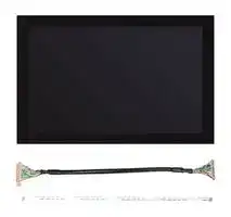
TFT LCD, 10.1 ", 1280 x 800 Pixels, WSXGA, Landscape, Black on White, 3.3V
⚠️ Reference pricing provided. In case of supply shortages, we will connect you with our trusted procurement partners to ensure your project's continuity.
- Manufacturer: TORADEX
- Product type: TFT LCD Displays
- SVHC: No SVHC (25-Jun-2025)
- VGA Size: WSXGA
- Resolution: 1280 x 800 Pixels
- Module Size: 248.5mm x 166.1mm
- Touchscreen: Capacitive Touch
- Display Size: 10.1"
- Logic Voltage: 3.3V
- Product Range: -
- Display Pinout: -
- Interface Type: LVDS, I2C
- Display Appearance: Black on White
- Display Brightness: 400cd/m²
- Display Orientation: Landscape
- Operating Temperature Max: 70°C
- Operating Temperature Min: -20°C
| Delivery and price | |
|---|---|
| Units per pack | 1 |
| Price | 338.17 € |
| Current stock | 10+ |
| Lead time | 30 days |
Datasheet

**Capacitive Touch Display 10.1" LVDS** Datasheet
Logic Technologies Part Number : LT170410-2WHC Issue Date : 31.07.2019 Version : 1.1
## **PRODUCT SPECIFICATION**
# **DESCRIPTION**
**TFT Module – 10.1” WSXGA 1280x (RGB) x 800 IPS Display with cap touch PART NUMBER LT170410-2WHC**
**VERSION 1.1 ROHS COMPLIANT**
2/27
Logic Technologies Part Number : LT170410-2WHC Issue Date : 31.07.2019 Version : 1.1
## **Revision Status**
|**Revision**|**Revision Date**|**Page**|**Content**|**Notes**|
|---|---|---|---|---|
||||||
|1.0|12.09.2018||Initial release||
|1.1|31.07.2019||1. Updated Schematics, Add C11 to<br>AP3012 for power sequence._Page13<br>2. Update the packaging drawing, add<br>10pinsFFCforCap touch_Page19||
||||||
||||||
||||||
||||||
||||||
||||||
||||||
||||||
||||||
||||||
||||||
||||||
||||||
||||||
||||||
||||||
||||||
||||||
||||||
||||||
||||||
||||||
||||||
||||||
||||||
||||||
||||||
||||||
||||||
**==> picture [515 x 104] intentionally omitted <==**
3/27
Logic Technologies Part Number : LT170410-2WHC Issue Date : 31.07.2019 Version : 1.1
## **Table of Contents**
**GENERAL INFORMATION** **MECHANICAL DIMENSIONS** **ABSOLUTE MAXIMUM RATINGS** **ELECTRICAL CHARACTERISTICS** **BACKLIGHT CHARACTERISTICS** **ELECTRO-OPTICAL CHARACTERISTICS** **INTERFACE DESCRIPTION** **BLOCK DIAGRAM** **TIMING CHARACTERISTICS** **TIMING CHART & DATA** **TOUCH PANEL CHARACTERISTICS** **RELIABILITY TESTING** **INSPECTION CRITERIA** **INSPECTION STANDARD** **PRECAUTIONS FOR USING LCD MODULES**
4/27
Logic Technologies Part Number : LT170410-2WHC Issue Date : 31.07.2019 Version : 1.1
## **GENERAL INFORMATION**
|**Item**|**Contents**|**Unit**|
|---|---|---|
|LCD Type|Transmissive TFT, normally Black|---|
|Technology|IPS TFT|-|
|Viewing Direction|Full View|O’clock|
|Module dimensions (W x H x T)|248.5x 166.1 x 15.0 ( Max* )|mm|
|Active area (W x H)|216.96 x 135.60|mm|
|Number of pixels|1280 x 3 (RGB) x 800|---|
|Pixel pitch (W x H)|(0.0565x3) x 0.1695|mm|
|Colours|16.7M|---|
|Contrast ratio|800:1 (typical)|---|
|Backlight|LED (36 dual core LEDs; 6 serial x 6)|---|
|Backlight Brightness|400|cd/m2|
|Interface|LVDS 8-bit|---|
|With Touch|CTP touch|---|
|Operating temperature|-20 to +70|°C|
|Storage temperature|-30 to +80|°C|
*Exclusive hooks, posts ,PCB/FFC/FPC tail etc, thickness is 6.9mm. Once including will be 15mm.
5/27
Logic Technologies Part Number : LT170410-2WHC Issue Date : 31.07.2019 Version : 1.1
## **MECHANICAL DIMENSIONS**
**==> picture [540 x 705] intentionally omitted <==**
**----- Start of picture text -----**<br>
1 66.10(CTP Outline)<br>6.50 1 49.10±0.30(LCD Module Outline) 1 0.50<br>6.5 1 49.85±0.30(Sensor Outline) 9.75<br>15.00 1 37.10(CTP Viewing Area) 1 4.00<br>15.70 1 35.60(LCD AA) 1 4.80<br>72.85<br>j Tiriria<br>4<br>ty<br>in !<br>A 1 t esoe<br>| Z<br>ry<br>ioyd<br>ie my ! !<br>' s o O , bd<br>ray<br>ry 9.75±0.20<br>'<br>q ~ ry1<br>;<br>79<br>i Toradex label<br>i<br>' 40 PCBA<br>- 20±1 Po 1<br>f r Cel -<br>ee<br>fi ri a<br>= [J] Tr<br>aC=O The area couldn't bend1.5Max H=<br>i]5@oo +L Far# aa!=<br>sO<br>Atmel mXT1066T2 4 ' f- e<br>tnt} i 82 Conductive Cloth i t<br>17.50 20±1<br>20.70<br>tt ty<br>T4<br>1<br>6.50±0.20 0.75(Sensor)<br>1 49.10±0.20(Sensor )<br>6/27<br>F E D C B A<br>Notes:<br>1 15.80 15.00 9.05 10.84 1<br>7.RoHS compliant<br>Mechanical Dimensions<br>1<br>8.General tolerance: ±0.3mm<br>Ink Printing: Black<br>2.Viewing direction:Full viewing 13.45<br>5.Logic power supply voltage:3.3V 1.Display type:10.1" IPS TFT with CTP LEDK LEDA<br>2 (1280 2<br>Storage temperature:-30degC~+80degC<br>4.Operation temperature:-20degC~+70degC 3.Polarizer mode:Transmissive/Normal black<br>)RGB<br>Backlight Circuit 216.96(LCD AA)<br>(6 dual core LEDs x 6) 8-bits LVDS I/F Full viewing Angle x800 With Capacitive TP 10.1" IPS TFT 218.46(CTP Viewing Area) 230.36±0.30(Sensor Outline) 248.46(CTP Outline)<br>229.50±0.30(LCD Module Outline)<br>Transmissive/Normal black<br>6.Backlight:White,VLED+=12V, Luminance: 400(typ.)cd/m2<br>Top Protected Film<br>3 PIN1 PIN30 CN1 3<br>1 1<br>25±5 8 5.70 5.00 9.05 8.13<br>20<br>250±10 20 AWG30 dirmeter wires 1 1 1<br>8 5.0 (Max) .90(CTP) 4.80(TFT) 6.90±0.30<br>Toradex carrier board LT170410-2WHC to LVDS cable from 25±5 1.50±0.30<br>PIN2 K PIN40 CN2 CN2: HRS DF13-40DS-1.25C, 40Pins female, Pitch:1.25, Twisted-pair<br>CN1: P-TWO INDUSTRIES INC FIX-30P-D8, 30PINS, Pitch 1.0, single row. 4<br>4 K Direction PIN1 PIN39 5 1 8.36±0.2<br>30 92 28 27 26 25 24 23 22 21 20 19 81 17 16 15 14 13 12 11 10 9 8 7 6 5 4 3 2 1 CN1<br>04 39 29 26 37 35 32 1-pair 3 02 25-pair 27 17 7-pair 9 14 31-pair 15 11 p19air- 21 5 32 32 2 CN2 Value Chart 3 0±1<br>Twisted Twisted Twisted Twisted Twisted Remarks Logic Label<br>GND<br>FPCB Inserting direction Ver F Ver E Ver D Ver C Ver B Ver A<br>1<br>LT170420-1PCBA Chan Chan<br>71.00±0.15 1 CON5 FH34SRJ-10S-0.5SH 101 1 230.36±0.2(Sensor) g g 5<br>5 First release<br>1 CON4-INPUT gCorrect the bri<br>71.92<br>20.00 PCBA Correct the CON4<br>30 p<br>11.74±0.50 V1.01 LT170410-2PCBA<br>IC<br>GND<br>LT170410-2WHC Part Number LOGIC 26.25 2±0.5 1 1.78(Sensor) e the LVDS cable notes. in 1~5 to NC<br>Not to scale. Unit mm.<br>9.05±0.20<br>6 10 9 8 7 6 5 4 3 2 1 PIN 30 29 28 27 26 25 24 23 22 21 20 19 18 17 16 15 14 13 12 11 10 9 8 7 6 5 4 3 2 1 (e the CTP connector to FH34SRJ-40S-0.5SH qMove the CTP connector to left side as customer re 6<br>Sheet: 1/1 F Revision TECHNOLOGIES NC NC NC NC 3.3V+ /RESET /INT GND I2C_SCL I2C_SDA SYMBOL CN5-INPUT CC/VLED+ CC/VLED+ VSS/LED- VSS/LED- _ ONBL _ BLPWM GND RxIN3+ RxIN3- GND RxCLKIN+ RxCLKIN- GND RxIN2+ RxIN2- GND RxIN1+ RxIN1- GND RxIN0+ RxIN0- GND VDD VDD GND NC NC NC NC NC CON4-INPUT )Hirose. uest.<br>htness on notice. Should 400cd/m2 after cover touch<br>F E D C B A<br>40<br>1<br>40<br>1<br>**----- End of picture text -----**<br>
Logic Technologies Part Number : LT170410-2WHC Issue Date : 31.07.2019 Version : 1.1
## **ABSOLUTE MAXIMUM RATING**
|**Parameter**|**Symbol**|**Min.**|**Max.**|**Unit**|**Note**|
|---|---|---|---|---|---|
|Power Voltage|VDD|- 0.3|3.9|V|---|
||VLED+|-0.3|16|V|--|
|Backlight LED Forward Current|IF|---|70|mA|One LED|
|Operating Temperature|TOPR|-20|70|°C|---|
|Storage temperature|TST|- 30|80|°C|---|
## **ELECTRICAL CHARACTERISTICS**
|**Parameter**|**Symbol**|**Min**|**Typ.**|**Max**|**Unit**|**Remark**|
|---|---|---|---|---|---|---|
|Supply Voltage|VDD|3.0|3.3|3.5|V|Note1|
|Input signal high voltage|VIH|0.8 VDD||VDD|V|Note2|
|Input signal low voltage|VIL|0||0.2VDD|V||
|Current for driver|IVDD||247|350|mA|VDD =3.3V|
Note 1: VDD setting should match the signals output voltage of customer’s system board.
Note2: Typical VCOM is only a reference value, it must be optimized according to each LCM. Be sure to use VR.
7/27
Logic Technologies Part Number : LT170410-2WHC Issue Date : 31.07.2019 Version : 1.1
## **BACKLIGHT CHARACTERISTICS**
|**Item**|**Symbo**<br>**l**|**Min.**|**Typ.**|**Max.**|**Unit**|**Condition**|
|---|---|---|---|---|---|---|
|Backlight Forward Voltage|VF|16.8|19.5|21|V|Notes|
|Backlight Forward Current|IF|200|240|280|mA||
|Driver Input Voltage|VLED+|9|12|15|||
|Driver Input Current|IVLED||438||||
|PWM Frequency|PWM|100|150|200|Hz||
|LED Lifetime|---|---|20000|---|Hrs||
|Power Consumption|WBL|---|5.3|---|W||
## NOTES:
## Backlight drive conditions: **constant current** driving method.
- The LED driving condition is defined for the module (6 dual core LED Serial x 6 Parallel).
- The LED driving condition is defined for total backlight consumption and the driver circuit.
- Forward Voltage adjustment depends on the Forward Current setting.
- One LED : max IF = 50mA, VF = 3.5V
- The LED lifetime is typically 20,000 hours at 25degC.
- IF =240mA is defined for all channels LEDs.
- If the LEDs are driven by high current, high ambient temperature & humidity condition the lifetime of the LEDs will be reduced.
- Operating life means brightness reduces to 50% of initial brightness and typical operating life time is estimated data.
8/27
Logic Technologies Part Number : LT170410-2WHC Issue Date : 31.07.2019 Version : 1.1
- **ELECTRO-OPTICAL CHARACTERISTICS**
|**Item**|**Item**|**Symbol**|**Condition**|**Min.**|**Typ.**|**Max.**|**Unit**|**Refer**|**Note**|
|---|---|---|---|---|---|---|---|---|---|
|Response Time||TON|25°C|---|10|20|ms|Fig 1|1|
|||TOFF||---|15|30||||
|Contrast ratio||Cr|°|600|800|---|---|Fig 2|1|
|Uniformity||U|---|70|80|---|%|Fig 2|3|
|Surface Luminance||Lv||330|400|---|cd/m2|Fig 2|2|
|Viewing angle ratio|||°|---|85|---|---|Fig 3|6|
||||°|---|85|---||||
||||0°|---|85|---||||
||||180°|---|85|---||||
|CIE (x,y)<br>chromaticity|Red|x|Backlight<br>On|0.530|0.580|0.630|---|Fig 2.|5|
|||y||0.300|0.350|0.400||||
||Green|x||0.270|0.320|0.370||||
|||y||0.550|0.600|0.650||||
||Blue|x||0.100|0.150|0.200||||
|||y||0.070|0.120|0.170||||
||White|x||0.260|0.310|0.360||||
|||y||0.280|0.330|0.380||||
Test Conditions: DVDD=3.3V, IL=480mA (Backlight current), the ambient temperature is 25 ℃ . Optical performance should be evaluated at Ta=25 ℃ only.
## NOTES
1. Contrast ratio (CR) is defined mathematically in Figure 2.
Contrast Ratio = Average Surface Luminance with all white pixels (P1, P2, P3, P4, P5) Average Surface Luminance with all black pixels (P1, P2, P3, P4, P5)
Note 2. Surface luminance is the LCD surface from the surface with all pixels displaying white. For more information see figure 2.
Lv = Average Surface Luminance with all white pixels (P1, P2, P3, P4, P5…)
Note 3. Uniformity of surface luminance, White, is defined mathematically in figure 2.
White = Minimum Surface Luminance with all white pixels (P1, P2, P3, P4, P5) Maximum Surface Luminance with all white pixels (P1, P2, P3, P4, P5)
Note 4. Response time is the time required for the display to transition form white to black (rise time Tr) and from black to white (decay or fall time, Tf). The industry standard test equipment used is the Autronic-Melcher’s Conoscope.
9/27
Logic Technologies Part Number : LT170410-2WHC Issue Date : 31.07.2019 Version : 1.1
Note 5. CIE (x,y) chromaticity. The x,y value is determined by measuring luminance at each test position 1 through 5, then calculating the average value.
Note 6. The Viewing angle is the angle at which the contrast ratio is greater than 2. For a TFT module, the contrast ratio is greater than 10. The angles are determined for the horizontal or ‘x’ axis and the vertical or ‘y’ axis with respect to the ‘z’ axis, being the LCD surface reference. Also see figure 3.
Note 7. For viewing angle and response time testing, the testing data is based on Autronic-Melcher’s BM-7A. For the contrast ratio, surface luminance, luminance uniformity and chromaticity (CIE), the test data is based on the industry’s standard SR-3A photo detector.
Note 8. For TFT modules, grey scale reversing occurs in the direction of the panel viewing angle.
Figure 1. Definition of response time
**==> picture [268 x 78] intentionally omitted <==**
**----- Start of picture text -----**<br>
> Tr + > Tf <<br>100%<br>90%<br>10%<br>0<br>white black white<br>Optical<br>Response<br>**----- End of picture text -----**<br>
Figure 2. Measuring contrast ratio, surface luminance, luminance uniformity and CIE (chromaticity).
A : 5mm, B : 5mm, H & V : Active area.
Light spot diameter =7mm, 500mm distance from the LCD surface to the detector lens. Measurement instrument is Topcon’s luminance meter BM-7.
**==> picture [173 x 108] intentionally omitted <==**
**----- Start of picture text -----**<br>
H<br>A A<br>(<br>en) nn wn<br>P1 P2<br>© P5<br>' P4 P3<br>B<br>V<br>B<br>**----- End of picture text -----**<br>
Figure 3. Definition of viewing angle
**==> picture [196 x 142] intentionally omitted <==**
**----- Start of picture text -----**<br>
θ=0<br>Up z<br>Φ=90<br>(12:00) θ<br>y<br>Φ<br>Left Right<br>Φ=180 x Φ=0<br>(9:00) (3:00)<br>Down<br>Φ=270<br>(6:00)<br>**----- End of picture text -----**<br>
10/27
Logic Technologies Part Number : LT170410-2WHC Issue Date : 31.07.2019 Version : 1.1
## **INTERFACE DESCRIPTION**
## **TFT 8-bit LVDS Interface**
|**Pin**|**Symbol**|**I/O**|**Description**|**Note**|
|---|---|---|---|---|
|1|NC|--|Not connect||
|2|NC|--|Not connect.||
|3|NC|--|Not connect||
|4|NC|--|Not connect||
|5|NC|--|Not connect||
|6|GND|P|Ground||
|7|VDD|P|TFT&CTP Power supply, 3.3V||
|8|VDD|P|TFT&CTP Power supply, 3.3V||
|9|GND|P|Ground||
|10|RxIN0-|I|Transmission Data of Pixels||
|11|RxIN0+|I|Transmission Data of Pixels||
|12|GND|P|Ground||
|13|RxIN1-|I|Transmission Data of Pixels 1||
|14|RxIN1+|I|Transmission Data of Pixels 1||
|15|GND|P|Ground||
|16|RxIN2-|I|Transmission Data of Pixels 2||
|17|RxIN2+|I|Transmission Data of Pixels 2||
|18|GND|P|Ground||
|19|RxCLKIN-|I|-LVDS differential clock input||
|20|RxCLKIN+|I|+LVDS differential clock input||
|21|GND|P|Ground||
|22|RxIN3-|I|Transmission Data of Pixels 3||
|23|RxIN3+|I|Transmission Data of Pixels 3||
|24|GND|P|Ground||
|25|BL_PWM|I|PWM signal to control backlight diming.<br>100~200Hz||
|26|BL_ON|I|Backlight on/off controlpin. H: On ; L: Off||
|27|VSS/LED-|P|Backlight Ground which is LED Cathode.||
|28|VSS/LED-|P|||
|29|VCC/LED+|P|Backlight supply voltage input, 12V typical||
|30|VCC/LED+|P|||
I -Input only; O -Output only; I/O -Input /output; P -Power or Ground.
11/27
Logic Technologies Part Number : LT170410-2WHC Issue Date : 31.07.2019 Version : 1.1
## **TP Interface**
|**Pin**|**Symbol**|**I/O**|**Description**|**Note**|
|---|---|---|---|---|
|1|I2C_SDA|I|I2C data input/output||
|2|I2C_SCL|I|I2C clock singal||
|3|GND|P|Ground||
|4|/INT|I|Wake up/Interrupt, equal to /CHG of Atmel<br>MXT1066T2||
|5|/RESET|I|Reset signal for CTP, low active.||
|6|+3.3V|P|3.3V supply power input||
|7|NC(CLK)|I|Not connection||
|8|NC(CS)|I|Not connection||
|9|NC(TX)|I|Not connection||
|10|NC(RX)|I|Not connection||
## **BLOCK DIAGRAM**
12/27
Logic Technologies Part Number : LT170410-2WHC Issue Date : 31.07.2019 Version : 1.1
## **Schematcis**
**==> picture [515 x 701] intentionally omitted <==**
**----- Start of picture text -----**<br>
13/27<br>CN5 CN4<br>12 11 10 9 8 7 6 5 4 3 2 1 34 33 32 31 30 29 28 27 26 25 24 23 22 21 20 19 18 17 16 15 14 13 12 11 10 9 8 7 6 5 4 3 2 1<br>FH34SRJ-10S-0.5SH VSS VSS 3.3V RST- INT VSS SCL SDA FI-X30SSLA-HF VIN VIN VSS VSS VSS VSS VSS VSS 3.3V 3.3V VSS<br>CTP VSS VSS/LED- VSS/LED- BL_ON BL_PWM RXIN3+ RXIN3- RXCLK+ RXCLK- RXIN2+ RXIN2- RXIN1+ RXIN1- RXIN0+ RXIN0-<br>0R R19 NC--100R R12 NC--100R R11 NC--100R R8 NC--100R R7 NC--100R R6<br>VSS<br>10UF/25V/1206 C7<br>3.3V<br>1UF C11 NC--0R R27 VCC 1K R16 ZD3<br>3.3V 4 5 0R R28 4.7K R18<br>100K R22 2K R23<br>U2 PTZTE2515B<br>VIN BL_PWM<br>/SHDN L2 VIN Q3<br>AP3012 100K R24 10K R5<br>FB GND SW<br>3 2 1 33UH/5D28 C4 MMS8550-2TY Q4 VCC S8 Q5 VCC<br>3.3K R21 56K R20 VSS/L 10UF/50V/1206 NCE55P15K 050-J3Y10K R26 10K R25<br>ED- D4 D2<br>IN5819<br>IN5819<br>D3 C2<br>C1<br>IN5819 VLED+ Backlight Brightness = 100% if PWM = 0<br>C8 VGH C5 BL_ON Backlight Brightness = 0% if PWM = 100%<br>+22V ZD1 10UF/50V/1206 10UF/50V/1206 1N5822 D1 10K R2<br>10UF/50V/1206 10UF/25V/1206 S8 Q1<br>PTZTE2515B<br>PTZTE2513B ZD2 C6 -7V VGL 050-J3Y 10K R4 10K R3 VCC<br>A<br>C9 VDD 10UF/25V/1206 3.3V 10K R9 C3 3.3V 33UH/5 L1 S8 Q2<br>D VSS/LE<br>8.2V 10K R10 SDA SCL 3.3V INT VSS 10UF/25V/1206 4 3 1 28 D- 050-J3Y 100R R13<br>3K R15 10UF/25V/1206 5.1K R14 RST-CTP NC VIN U3 1R R17 VLED- VC<br>C<br>VCOM 6 5 4 3 2 1 J4 ON/OFF R1 5 4 3 2 1<br>FPC1.0-2-6P<br>上接 ME6211C25M5G VSS VOUT NC--0R FB VIN SW EN GND U1<br>XL6005<br>2 5<br>Date: D Size Title VDD<br>C10<br>29Nov-- Number 10UF/25V/1206<br>2018<br>File: LT170410-1PCBA Sch v1.03<br>VSS VSS VLED+ VLED+ VGH VGL VLED- VLED- VSS AVDD VSS VSS RXIN3+ RXIN3- VSS RXCLK+ RXCLK- VSS RXIN2+ RXIN2- VSS RXIN1+ RXIN1- VSS RXIN0+ RXIN0- VSS VDD VDD VCOM CN1<br>42 41 40 39 38 37 36 35 34 33 32 31 30 29 28 27 26 25 24 23 22 21 20 19 18 17 16 15 14 13 12 11 10 9 8 7 6 5 4 3 2 1<br>Drawn By: Sheet of<br>0.5K-AS-40PWB(0.5MM-40P<br>Revision 上抽)<br>**----- End of picture text -----**<br>
Logic Technologies Part Number : LT170410-2WHC Issue Date : 31.07.2019 Version : 1.1
## **TIMING CHARACTERISTICS**
LVDS mode AC electrical characteristics
14/27
Logic Technologies Part Number : LT170410-2WHC Issue Date : 31.07.2019 Version : 1.1
## Timing Table
15/27
~~OO~~ Logic Technologies Part Number : LT170410-2WHC Issue Date : 31.07.2019 Version : 1.1
LVDS data input format
## 8-bit LVDS data input
16/27
Logic Technologies Part Number : LT170410-2WHC Issue Date : 31.07.2019 Version : 1.1
## Power on/Off sequence
## Power On
Power Off sequence
17/27
Logic Technologies Part Number : LT170410-2WHC Issue Date : 31.07.2019 Version : 1.1
## **TOUCH PANEL CHARACTERISTICS**
**CONSTRUCTION – Lens + OCA + Seneor(ITO glass) + FPC (See Note 1)**
|**Item**|**Symbol**|**Min.**|**Typ.**|**Max.**|**Unit**|**Note**|
|---|---|---|---|---|---|---|
|Overall dimensions|---|248.5 x 166.1 x 1.9|||mm||
|Viewing Area|---|218.5 x 137.1|||mm||
|Total Thickness|---|---|1.90|---|mm|+/- 0.15mm|
|Lens thickness|---|---|1.1|---|mm|+/- 0.15mm|
|OCA thickness|---|---|0.15|---|mm|+/- 0.05mm|
|Sensor thickness|---|---|0.55|---|mm|+/- 0.05mm|
|Lens surface hardness|---|6|---|---|H|JIS K 5600|
## Note 1
- (i) Lens = 6H surface hardness + black mask area
- (ii) OCA = Optically Clear Adhesive
- (iii) ITO = Indium Tin Oxide (touch sensor layer)
- (iv) FPC = Flexible Printed Circuit (includes Atmel Mxt1066T2 controller IC)
The minimum test force is 80g.
## **TOUCH PANEL INTERFACING (Connector CN2)**
|**Pin No**|**Symbol**|**I/O**|**Description**|**Note**|
|---|---|---|---|---|
|1|GND|P|Ground||
|2|/CHG INT|I|External Interrupt to the host||
|3|/RESET|I|External Interrupt from the host||
|4|VDD_3.3V|P|CTPpower supply(+3.3V)||
|5|SCL|I/O|I2C clock input||
|6|SDA|I/O|I2C data input and output||
## TOUCH PANEL BLOCK DIAGRAM
18/27
Logic Technologies Part Number : LT170410-2WHC Issue Date : 31.07.2019 Version : 1.1
**==> picture [501 x 746] intentionally omitted <==**
**----- Start of picture text -----**<br>
<br>PACKAGE DRAWING<br>+<br>1 66.1<br>Toradex label<br>: ee<br>| iii<br>—<br>go<br>,<br>| | Conductive Cloth b a a<br>2 63<br>, tT<br>Toradex label<br>x<br>ac<br>g o at<br>Zz < Conductive Cloth :<br>—<br>a)<br>+<br>19/27<br>240<br>321<br>F E D C B A<br>B<br>10 1<br>5 4 3 2 1<br>NO.<br>1 1<br>Logic<br>Label<br>Module Content GND<br>LVDS cable Logic label 2<br>Toradex 10.1" label Bubble ESD bag Module 50 10pins FFC LT170420-1PCBA CON5 FH34SRJ-10S-0.5SH 101 248.46 1<br>Mechanical Dimensions<br>Qty V1.01 LT170410-2PCBA<br>12PCS 24PCS 24PCS 12PCS 12PCS<br>GND<br>2 9 8 7 6 NO. MADE G.W N.W Q'ty 10 1 2<br>IN<br>5 5.0 (Max) 1<br>CHINA<br>Outer Box Foam cover Content : ........................KG : ........................KG : .....................PCS PartNO: .............................<br>Black inner box<br>4<br>10Pins FFC-YM-0510250A 00<br>2<br>3 1PC 2PCS 12PCS 12PCS Qty 3<br>Put in outer box and seal<br>B Size: 240x330x8 Bubble ESD Bag<br>B<br>10 1<br>4 4<br>Put in inner box<br>Seal the bag gate Logic<br>Label<br>GND<br>10pins FFC LT170420-1PCBA 3<br>CON5 FH34SRJ-10S-0.5SH 101<br>C B A<br>V1.01 LT170410-2PCBA<br>5 GND 5<br>10 1 First release<br>Part Number<br>LOGIC<br>LT170410-2WHC package<br>4<br>Not to scale. Unit mm.<br>6 6<br>Add the 10pins FFC cable for Cap touch connection<br>B<br>Sheet: 1/1 Revision on bag top side<br>TECHNOLOGIES<br>Add Toradex label<br>F E D C B A<br>290<br>250±10<br>**----- End of picture text -----**<br>
Logic Technologies Part Number : LT170410-2WHC Issue Date : 31.07.2019 Version : 1.1
Note: Bubble ESD bag and packaging steps.
- 1). Bubble ESD Bag 2). Insert Display
3). Seal the gate with tape 4). Add the label on top
5). Put the module and LVDS cable into inner box
20/27
Logic Technologies Part Number : LT170410-2WHC Issue Date : 31.07.2019 Version : 1.1
## **RELIABILITY TESTING**
|**NO.**|**Item**|**Condition**|**Criteria**|
|---|---|---|---|
|1|High Temperature Operating|70°C +/-2°C, 240Hrs|IEC60068-2-1, GB2423.2|
|2|Low Temperature Operating|-20°C +/-2°C, 240Hrs|IEC60068-2-1<br>GB2423.1|
|3|High Temperature Storage|80°C +/-2°C, 240Hrs|IEC60068-2-1<br>GB2423.2|
|4|Low Temperature Storage|-30°C +/-2°C, 240Hrs|IEC60068-2-1<br>GB2423.2|
|5|Hi Temperature & High Humidity<br>Operation|50°C, 90%RH max, 240Hrs|IEC60068-2-78<br>GB/T2423.3|
|6|Vibration<br>(non operating)|Vibration<br>Frequency range:10~55Hz,<br>Stroke:1.5mm Sweep:10Hz~<br>55Hz~10Hz2hours for each<br>directionof x.y.z(6hoursfortotal)|IEC60068-2-6<br>GB/T2423.10|
|7|Package Vibration Test|Random Vibration:<br>0.015GxG/Hz for 5-200Hz,<br>-6dB/Octave from 200-500Hz<br>2 hours for each direction of X,Y,Z<br>(6hoursfortotal)|IEC60068-2-34<br>GB/T2423.11|
|8|Thermal Shock<br>(non operating)|-20°C to 30min to 70°C, 30min<br>Change time: 5min, 10 cycles|Start with cold temperature,<br>End with high temperature,<br>IEC60068-2-<br>14:1984,GB2423.22|
|9|Drop Test<br>(packaged)|Height:80 cm,1 corner, 3 edges, 6<br>surfaces|IEC60068-2-32<br>GB/T2423.8|
|10|Shock (non-operation)|80G 6ms, ±X,±Y,±Z 3 times for<br>each direction|IEC60068-2-27<br>GB/T2423.5|
|11|ESD (operation)|C=150pF,R=330Ω,<br>Air:±15Kv, Contact:±8Kv,<br>10times/terminal|IEC61000-4-2<br>GB/T17626.2|
## Notes:
1. Test samples are applied to one test item.
2. Samples for each test item are 2-10pcs.
3. For humidity testing, a pure water resistance of >10MW
4. (a) In the case of a malfunction caused by ESD damage, if the LCM returns to normal state after reset, the item is considered to have passed the ESD test.
- (b) It is recommended to use an anti-static blower (ioniser) to reduce the electro-static voltage in the working area.
- (c) When removing the protection film from the TFT panel, peel off the film slowly (more than 1sec) while blowing the ioniser towards the peeling area to minimize ESD. This will reduce the risk of damaging the electrical circuitry.
5. In operating test, please use the automatic pictures changes test mode or automatic pictures changes on demonstration box.
21/27
Logic Technologies Part Number : LT170410-2WHC Issue Date : 31.07.2019 Version : 1.1
## **INSPECTION CRITERIA**
This specification is designed to be used as the standard acceptance/rejection criteria for normal LCM products.
## 1. Sampling plan.
The sampling plan according to GB/T 2828.1-2003 / ISO2859-16 1999 and ANSI/ASQC Z1.4 1993, normal level 2 and based on:
- Major defect: AQL 0.65
- Minor defect: AQL 1.5
## 2. Inspection condition
- The viewing distance for cosmetic inspection is approximately 30cm with the naked eye, and under an environment of 20-40W light intensity, in all directions, within 45° against a perpendicular line. (Normal temperature 20-25°C and normal humidity 60+/-15 RH.)
- Driving voltage - The Vop value from which the most optimal contrast can be obtained near the specified Vop in the specification (within +/-0.5V of the typical value at 25°C.)
3. Definition of inspection zone in LCD.
Figure 4
Zone A : Active Area Zone B : Viewing Area except Zone A (Zone A + Zone B = Minimum viewing area) Zone C : Outside Viewing Area (invisible area after assembling A B C into customer’s product.
Figure 4 inspection zones in an LCD
Note: As a general rule visual defects in Zone C are permissible when there is no visual effect once assembled into the customer’s product.
## **INSPECTION STANDARD**
MAJOR CRITERIA
Item No Item to be inspected Inspection standard Classification 1) No display 2) Display abnormal 1 All functional defects 3) Missing vertical or horizontal segment 4) Short circuit 5) Backlight not working, flickering and abnormal light Major 2 Missing Missing component Overall outline dimension beyond the drawing 3 Outline dimension dimension is not allowed ~~tO~~
22/27
Logic Technologies Part Number : LT170410-2WHC Issue Date : 31.07.2019 Version : 1.1
## COSMETIC CRITERIA
|No.|Item|Judgment Criteria|Partition|
|---|---|---|---|
|1|Difference in Spec.|None allowed|Major|
|2|Patternpeeling|No substratepatternpeelingand floating|Major|
|3|Soldering defects|No soldering missing<br>No soldering bridge<br>No cold soldering|Major<br>Major Minor|
|4|Resist flaw on substrate|Invisible copper foil(0.5mm or more)on substratepattern|Minor|
|5|Accretion of metallic Foreign<br>matter|No soldering dust<br>No accretion of metallic foreign matters(Not exceed0.2mm)|Minor<br>Minor|
|6|Stain|No stain to spoil cosmetic badly|Minor|
|7|Plate discoloring|Noplate fading,rustingand discoloring|Minor|
|8|Solder amount<br>1. Lead parts|a. Soldering side of PCB<br>Solder to form a ‘Filet’<br>all around the lead.<br>Solder should not hide the<br>lead form perfectly. (too much)<br>b. Components side<br>( In case of ‘Through Hole PCB’ )<br>Solder to reach the Components side of PCB.|Minor|
||2. Flat packages|Either ‘toe’ (A) or ‘heal’ (B) of<br>the lead to be covered by ‘Filet’.<br>Lead form to be assume<br>over solder.<br>A<br>B|Minor|
||3. Chips|(32) Hh(12) H<br>H<br>h|Minor|
|9|Solder ball/solder splash|a) The spacing between solder ball and the conductor or solder pad h<br>0.13mm.<br>The diameter of the solder ball d0.15mm.<br>b) The quantity of solder balls or solder splashes isn’t more than<br>5 in 600mm2.<br>c) Solder balls / splashes do not violate minimum electrical clearance<br>d) Solder balls/splashes must be not be able to be dislodged with<br>normalproduct usage|Minor<br>Minor<br>Major<br>Minor|
## COSMETIC CRITERIA (non-operating)
|No.|Defect|Judgment Criteria|Judgment Criteria|Judgment Criteria|Classification|
|---|---|---|---|---|---|
|1|Spots|In accordance with Screen Cosmetic Criteria(Operating)No.1.|||Minor|
|2|Lines|In accordance with Screen Cosmetic Criteria(Operating)No.2.|||Minor|
|3|Bubbles in polarizer|||AcceptableQtyin active area<br>Disregard<br>3<br>1<br>0|Minor|
||||Size : d mm|AcceptableQtyin active area||
||||d0.3<br>0.3d1.0<br>1.0d1.5<br>1.5d|Disregard<br>3<br>1<br>0||
|||||||
|4|Scratch|In accordance with spots and lines operating cosmetic criteria. When the light<br>reflects on thepanel surface,the scratches are not to be remarkable.|||Minor|
|5|Allowable density|Above defects should be separated more than 30mm each other.|||Minor|
|6|Coloration|Not to be noticeable coloration in the viewing area of the LCD panels.<br>Back-lit type should bejudged with back-lit on state only.|||Minor|
|7|Contamination|Not to be noticeable.|||Minor|
23/27
Logic Technologies Part Number : LT170410-2WHC Issue Date : 31.07.2019 Version : 1.1
## COSMETIC CRITERIA (operating)
|No.|Defect|Judgment Criteria|Judgment Criteria|Judgment Criteria|Classification|
|---|---|---|---|---|---|
|1|Spots|A) Clear<br>Note : Including pin holes and<br>size.<br>B) Unclear<br>Size : d mm<br>d0.1<br>0.1d0.2<br>0.2d0.3<br>0.3d<br>Size : d mm<br>d0.2<br>0.2d0.5<br>0.5d0.7<br>0.7d||defective dots which must be within one pixel<br>AcceptableQtyin active area<br>Disregard<br>6<br>2<br>0<br>AcceptableQtyin active area<br>Disregard<br>6<br>2<br>0|Minor|
||||Size : d mm|AcceptableQtyin active area||
||||d0.2<br>0.2d0.5<br>0.5d0.7<br>0.7d|Disregard<br>6<br>2<br>0||
|||||||
|2|Lines|A) Clear<br>Note :( )<br>- Acceptable Qty in active area<br>L<br>- Length (mm)<br>W<br>- Width (mm)<br><br>- Disregard<br>B) Unclear<br>2.0<br>L 10.0<br>See No. 1<br><br>(6)<br>(0)<br>W<br>0.5<br>0.3<br>0.05<br>2.0<br>L 5.0<br>See No. 1<br><br>(6)<br>(0)<br>W<br>0.1<br>0.05<br>0.02|||Minor|
|3|Rubbingline|Not to be noticeable.||||
|4|Allowable density|Above defects should be separated more than 10mm each other.|||Minor|
|5|Rainbow|Not to be noticeable.|||Minor|
|6|Dot size|To be 95 105of the dot size (Typ.) in drawing.<br>Partial defects of each dot (ex. pin-hole) should be treated as ‘spot’.<br>(see Screen Cosmetic Criteria(Operating)No.1)|||Minor|
24/27
**==> picture [518 x 238] intentionally omitted <==**
**----- Start of picture text -----**<br>
Logic Technologies Part Number : LT170410-2WHC Issue Date : 31.07.2019 Version : 1.1<br>7 Uneven brightness Uneven brightness must be BMAX BMIN 2 Minor<br>(only back-lit type - BMAX : Max. value by measure in 5 points<br>module) - BMIN : Min. value by measure in 5 points<br>Divide active area into 4 vertically and horizontally.<br>Measure 5 points shown in the following figure.<br> <br><br> <br> : Measuring points<br>**----- End of picture text -----**<br>
## Note :
- (1) Size : d = (long length short length) 2
- (2) The limit samples for each item have priority.
- (3) Complex defects are defined item by item, but if the number of defects are defined in above table, the total number should not exceed 10. (4) In case of ‘concentration’, even the spots or the lines of ‘disregarded’ size should not allowed.
## Following three situations should be treated as ‘concentration’.
- 7 or over defects in circle of 5mm.
- 10 or over defects in circle of 10mm.
- 20 or over defects in circle of 20mm.
## **PRECAUTIONS FOR USING LCD MODULES**
## **HANDLING PRECAUTIONS**
- (1) The display panel is made of glass. Do not subject it to a mechanical shock by dropping it or impact. (2) If the display panel is damaged and the liquid crystal substance leaks out, be sure not to get any in your mouth. If the substance contacts your skin or clothes, wash it off using soap and water. (3) Do not apply excessive force to the display surface or the adjoining areas since this may cause the color tone to vary. (4) The polarizer covering the display surface of the LCD module is soft and easily scratched. Handle this polarizer carefully. (5) If the display surface becomes contaminated, breathe on the surface and gently wipe it with a soft dry cloth. If it is heavily contaminated, moisten cloth with one of the following solvents: - Isopropyl alcohol - Ethyl alcohol
- (6) Solvents other than those above-mentioned may damage the polarizer. Especially, do not use the following. - Water - Ketone
- Aromatic solvents
(7) Exercise care to minimize corrosion of the electrode. Water droplets, moisture condensation or current flow in a high-humidity environment, accelerate corrosion of the electrodes.
25/27
Logic Technologies Part Number : LT170410-2WHC Issue Date : 31.07.2019 Version : 1.1
- (8) Install the LCD Module by using the mounting holes. When mounting the LCD module ensure it is free of twisting, warping or distortion.
- (9) Do not attempt to disassemble the LCD module.
- (10) NC terminal should be open. Do not connect anything.
- (11) If the logic circuit power is off, do not apply the input signals. (12) To prevent destruction of the elements by static electricity, be careful to maintain an optimum work environment.
- Be sure to ground the body when handling the LCD modules.
- Tools required for assembling, such as soldering irons, must be properly grounded.
- To reduce the amount of static electricity generated, do not conduct assembling and other
- work under dry conditions. - The LCD module is coated with a film to protect the display surface. Exercise care when peeling off this protective film since static electricity may be generated.
## **STORAGE PRECAUTIONS**
When storing the LCD modules, the following precaution is necessary.
- (1) Store them in a sealed polyethylene bag. If properly sealed, there is no need for the dessicant.
- (2) Store them in a dark place. Do not expose to sunlight or fluorescent light, keep the temperature between 0°C and 35°C, and keep the relative humidity between 40%RH and 60%RH.
- (3) The polarizer surface should not come in contact with any other objects. (We advise you to store them in the anti-static electricity container in which they were shipped.
## **OTHERS**
Liquid crystals solidify under low temperature (below the storage temperature range) leading to defective orientation or the generation of air bubbles (black or white). Air bubbles may also be generated if the module is subject to a low temperature.
If the LCD modules have been operating for a long time showing the same display patterns, the display patterns may remain on the screen as ghost images and a slight contrast irregularity may also appear. A normal operating status can be regained by suspending use for some time. It should be noted that this phenomenon does not adversely affect performance reliability.
To minimize the performance degradation of the LCD modules resulting from destruction caused by static electricity etc., exercise care to avoid holding the following sections when handling the modules.
- Exposed area of the printed circuit board.
- Terminal electrode sections.
## **PRECAUTIONS FOR SOLDERING THE LCM**
||ManualSoldering|MachineDrag Soldering|MachinePre-soldering|
|---|---|---|---|
|Non<br>ROHS<br>Product|290°C ~ 350°C<br>Speed : 3 ~ 5 mm/s|330°C ~ 350°C<br>Speed : 4 ~ 8mm/s|300°C ~ 330°C<br>Time : 3 ~ 6S<br>Pressure:0.8 to1.2Mpa|
|RoHS<br>Product|340°C ~ 370°C<br>Time : 3 ~ 5S.|350°C ~ 370°C<br>Time : 4 ~ 8 mm/S.|330°C ~ 360°C<br>Time : 3 ~ 6S.<br>Pressure:0.8~ 1.2Mpa.|
- (1) If solder flux is used, be sure to remove any remaining flux after finishing the soldering process. (This does not apply in the case of a non-halogen type of flux.) It is recommended that your protect the LCD surface with a cover during the soldering process to prevent any damage due to the flux sparks.
- (2) When soldering a backlight panel and PCB, the panel and PCB should not be detached more than 3 times. The temperature determines this number and time conditions as mentioned in the above table, although there may be some variance depending on the actual temperature of the soldering iron.
26/27
Logic Technologies Part Number : LT170410-2WHC Issue Date : 31.07.2019 Version : 1.1
- (3) When removing a backlight panel from the PCB, ensure the solder has completely melted, otherwise the solder pads on the backlight panel and/or PCB may be damaged.
## **OPERATION CAUTION**
(1) It is recommended to drive LCDs within their specified voltage limit since the higher voltage than the upper limit shortens the LCD life. An electrochemical reaction due to direct current causes the LCD to deteriorate. Therefore, avoid the use of direct current drive.
(2) Response time will be extremely delayed at lower temperatures than the operating temperature range. At higher temperatures LCD’s will experience a dark color. However those phenomena do not mean a malfunction or the LCD’s. Once the LCDs are returned to the specified operating temperature range, the response time and colouration should return to the normal state.
(3) If the display area is physically pressed hard during it’s operation, some pixels may be abnormally displayed, but should return to their normal condition after resetting the LCM.
(4) Moisture sitting on the LCM terminals is a cause for an electro-chemical reaction resulting in a terminal open circuit. Usage under the relative condition of 40°C, 50%RH or less is therefore required.
## **SAFETY**
- (1) It is recommended to crush any damaged or unnecessary LCDs into pieces and wash off the liquid crystal by using solvents such as acetone and ethanol, which should then be burned up later.
- (2) When any liquid crystal has leaked out of a damaged glass cell and comes in contact with skin, please wash it off well with soap and water.
## **RETURNING PRODUCTS UNDER WARRANTY**
No warranty can be granted if the precautions stated above have been disregarded. The typical examples of violations are:
- Broken LCD glass.
- PCB eyelet’s damaged or modified.
- PCB conductors damaged.
- Circuit modified in any way, including addition of components.
- PCB tampered with by grinding, engraving or painting varnish.
- Soldering to or modifying the bezel in any manner.
Product repairs will be invoiced to the customer upon mutual agreement. Products must be returned with sufficient description of the failures and/or defects. Any connectors or cable installed by the customer must be removed completely without damaging the PCB eyelet’s, conductors and terminals.
27/27
Capacitive Touch Display 10.1" LVDS Datasheet Disclaimer
## **DISCLAIMER**
Copyright © Toradex AG. All rights are reserved. The information and content in this document are provided “as-is” with no warranties of any kind and are for informational purposes only. Data and information have been carefully checked and are believed to be accurate; however, no liability or responsibility for any errors, omissions or inaccuracies is assumed.
Brand and product names are trademarks or registered trademarks of their respective owners. Specifications are subject to change without notice.
Toradex AG _·_ Ebenaustrasse 10 _·_ 6048 Horw _·_ Switzerland _·_ +41 41 500 48 00 _·_ www.toradex.com _·_ info@toradex.com
Page 27
Updated at April 23, 2026
About Novapart
Novapart is a B2B electronic component broker specialising in stock shortages and cost reduction. We source hard-to-find parts and identify compliant alternatives across a catalogue of 410,000+ components from 500+ manufacturers.
Learn more →Stock Shortage Specialist
When a component is unavailable, discontinued or has an unacceptable lead time, we tap into our network of vetted European and Asian distributors to source what you need — without compromising on quality or traceability.
Request a quote →Compliant Alternatives
We identify pin-to-pin, electrically equivalent substitutes that meet the same certifications (RoHS, AEC-Q100, REACH) as your original specification — validated against datasheets, not just part numbers. Often at a lower cost.
BOM Analysis service →