
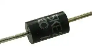


1.5KE16CA
TVS Diode, 1.5KE Series, Bidirectional, 13.6 V, 22.5 V, DO-201, 2 Pins
- Manufacturer: LITTELFUSE
- Product type: TVS Diodes
- SVHC: To Be Advised
- No. of Pins: 2Pins
- TVS Polarity: Bidirectional
- Product Range: 1.5KE Series
- Qualification: -
- Diode Mounting: Through Hole
- Diode Case Style: DO-201
- Clamping Voltage Max: 22.5V
- Reverse Standoff Voltage: 13.6V
- Maximum Breakdown Voltage: 16.8V
- Minimum Breakdown Voltage: 15.2V
- Operating Temperature Max: 175°C
- Peak Pulse Power Dissipation: 1.5kW
| Delivery and price | |
|---|---|
| Units per pack | 1000 |
| Price | 0.261 € |
| Current stock | 1000+ |
| Lead time | 30 days |
**TVS Diodes** Axial Leaded – 1500W > 1.5KE series

~~**RoHS** Pb~~ ~~**e3** HFL_IWAOO~~

## 1.5KE Series

## **Description** ~~es~~

**==> picture [49 x 7] intentionally omitted <==**

**----- Start of picture text -----**<br>
Uni-directional<br>**----- End of picture text -----**<br>


The 1.5KE Series is designed specifically to protect sensitive electronic equipment from voltage transients induced by lightning and other transient voltage events.

## **Features**

**==> picture [245 x 156] intentionally omitted <==**

**----- Start of picture text -----**<br>
Bi-directional<br>Agency Approvals<br>LE<br>Agency Agency File Number<br>E230531<br>a<br>Maximum Ratings and Thermal Characteristics<br>(TA=25 [O] C unless otherwise noted)<br>**----- End of picture text -----**<br>


**==> picture [233 x 166] intentionally omitted <==**

**----- Start of picture text -----**<br>
Parameter Symbol Value Unit<br>Peak Pulse Power Dissipation (Fig.2) by<br>10/1000μs Test Waveform (Fig.4) (Note 1)  PPPM 1500 W<br>-<br>Single Die Parts<br>Peak Pulse Power Dissipation(Fig.2) by<br>10/1000μs Test Waveform(Fig.4)(Note 1)  PPPM 2000 W<br>-Stacked Die Parts (Note 4)<br>Steady State Power Dissipation on Infinite Heat Sink at TL=75ºC  PD 6.5 W<br>Peak Forward Surge Current, 8.3ms Single Half Sine Wave Unidirectional Only (Note 2) IFSM 200 A<br>Maximum Instantaneous Forward Voltage at 100A for Unidirectional Only (Note 3) VF 3.5/5.0 V<br>Operating Junction and Storage Temperature Range TJ,  TSTG -55 to 175 °C<br>Typical Thermal Resistance Junction to Lead RθJL 15 °C/W<br>Typical Thermal Resistance Junction to Ambient RθJA 75 °C/W<br>**----- End of picture text -----**<br>


**Notes:**

**1.** Non-repetitive current pulse , per Fig. 4 and derated above TJ (initial) =25[O] C per Fig. 3.

**2.** Measured on 8.3ms single half sine wave or equivalent square wave, duty cycle=4 per minute maximum.

**3.** VF < 3.5V for single die parts and VF< 5.0V for stacked-die parts.

**4.** For stacked die component details, please refer to part numbers labeled by * in Electrical Characteristics.

**Functional Diagram** Po

**==> picture [172 x 55] intentionally omitted <==**

**----- Start of picture text -----**<br>
Bi-directional<br>Cathode  Anode<br>Uni-directional<br>**----- End of picture text -----**<br>


- 1500W peak pulse • Low incremental surge capability at 10/1000μs resistance waveform, repetition rate • Typical IR less than 1μA (duty cycles):0.01% when VBR min>12V

- Glass passivated chip • High temperature junction in DO-201 to reflow soldering Package guaranteed: 260°C/30sec

- • Fast response time: / 0.375”,(9.5mm) lead typically less than 1.0ps length, 5 lbs., (2.3kg) from 0 Volts to BV min tension

- Excellent clamping •  VBR @ TJ= VBR@25°C capability x (1+ **α** T x (TJ - 25))

- •  Typical failure mode is ( **α** T:Temperature short from over-specified Coefficient, typical value voltage or current is 0.1%)

- Whisker test is conducted • Plastic package is based on JEDEC flammability rated V-0 per JESD201A per its table 4a Underwriters Laboratories and 4c • Matte tin lead–free plated

- •  IEC-61000-4-2 ESD • Halogen free and RoHS 30kV(Air), 30kV (Contact) compliant

- ESD protection of data • Pb-free E3 means 2nd lines in accordance with level interconnect is IEC 61000-4-2 Pb-free and the terminal

- •  EFT protection of data finish material is tin(Sn) lines in accordance with (IPC/JEDEC J-STDIEC 61000-4-4 609A.01)

## **Applications** es,

TVS devices are ideal for the protection of I/O interfaces, VCC bus and other vulnerable circuits used in telecom, computer, industrial and consumer electronic applications.

## **Additional Infomarion**

**==> picture [171 x 8] intentionally omitted <==**

**----- Start of picture text -----**<br>
Datasheet Resources Samples<br>**----- End of picture text -----**<br>


© 2020 Littelfuse, Inc. Specifications are subject to change without notice. Revised: JC.10/30/20

**TVS Diodes** Axial Leaded – 1500W > 1.5KE series

## **Electrical Characteristics (TA=25°C unless otherwise noted)**

**==> picture [505 x 487] intentionally omitted <==**

**----- Start of picture text -----**<br>
Maximum<br>Maximum  Agency<br>Part   Part   Reverse Stand  Breakdown Voltage VBR Test   Clamping  Maximum Peak  Reverse  Approval<br>Number (Uni) Number (Bi) off Voltage V(Volts) R (Volts) @ IT Current  IT (mA) VVoltage C @  Ipp Pulse Current Ipp  (A) Leakage I(µA)R @ VR<br>Min. Max. (Volts)<br>1.5KE6.8A 1.5KE6.8CA 5.80 6.45 7.14 10 10.5 144.8 1000 X<br>1.5KE7.5A  1.5KE7.5CA 6.40 7.13 7.88 10 11.3 134.5 500 X<br>1.5KE8.2A  1.5KE8.2CA 7.02 7.79 8.61 10 12.1 125.6 200 X<br>1.5KE9.1A  1.5KE9.1CA 7.78 8.65 9.50 1 13.4 113.4 50 X<br>1.5KE10A  1.5KE10CA  8.55 9.50 10.50 1 14.5 104.8 10 X<br>1.5KE11A  1.5KE11CA  9.40 10.50 11.60 1 15.6 97.4 5 X<br>1.5KE12A  1.5KE12CA  10.20 11.40 12.60 1 16.7 91.0 5 X<br>1.5KE13A  1.5KE13CA  11.10 12.40 13.70 1 18.2 83.5 1  X<br>1.5KE15A  1.5KE15CA  12.80 14.30 15.80 1 21.2 71.7 1 X<br>1.5KE16A  1.5KE16CA  13.60 15.20 16.80 1 22.5 67.6 1 X<br>1.5KE18A  1.5KE18CA  15.30 17.10 18.90 1 25.2 60.3 1 X<br>1.5KE20A  1.5KE20CA  17.10 19.00 21.00 1 27.7 54.9 1 X<br>1.5KE22A  1.5KE22CA  18.80 20.90 23.10 1 30.6 49.7 1 X<br>1.5KE24A  1.5KE24CA  20.50 22.80 25.20 1 33.2 45.8 1 X<br>1.5KE27A  1.5KE27CA  23.10 25.70 28.40 1 37.5 40.5 1 X<br>1.5KE30A  1.5KE30CA  25.60 28.50 31.50 1 41.4 36.7 1 X<br>1.5KE33A  1.5KE33CA  28.20 31.40 34.70 1 45.7 33.3 1 X<br>1.5KE36A  1.5KE36CA  30.80 34.20 37.80 1 49.9 30.5 1 X<br>1.5KE39A  1.5KE39CA  33.30 37.10 41.00 1 53.9 28.2 1 X<br>1.5KE43A  1.5KE43CA  36.80 40.90 45.20 1 59.3 25.6 1 X<br>1.5KE47A  1.5KE47CA  40.20 44.70 49.40 1 64.8 23.5 1 X<br>1.5KE51A  1.5KE51CA  43.60 48.50 53.60 1 70.1 21.7 1 X<br>1.5KE56A  1.5KE56CA  47.80 53.20 58.80 1 77.0 19.7 1 X<br>1.5KE62A  1.5KE62CA  53.00 58.90 65.10 1 85.0 17.9 1 X<br>1.5KE68A  1.5KE68CA  58.10 64.60 71.40 1 92.0 16.5 1 X<br>1.5KE75A  1.5KE75CA  64.10 71.30 78.80 1 103.0 14.8 1 X<br>1.5KE82A  1.5KE82CA  70.10 77.90 86.10 1 113.0 13.5 1 X<br>1.5KE91A  1.5KE91CA  77.80 86.50 95.50 1 125.0 12.2 1 X<br>1.5KE100A  1.5KE100CA  85.50 95.00 105.00 1 137.0 11.1 1 X<br>1.5KE110A  1.5KE110CA  94.00 105.00 116.00 1 152.0 10.0 1 X<br>1.5KE120A  1.5KE120CA  102.00 114.00 126.00 1 165.0 9.2 1 X<br>1.5KE130A  1.5KE130CA  111.00 124.00 137.00 1 179.0 8.5 1 X<br>1.5KE150A  1.5KE150CA  128.00 143.00 158.00 1 207.0 7.3 1 X<br>1.5KE160A  1.5KE160CA  136.00 152.00 168.00 1 219.0 6.9 1 X<br>1.5KE170A  1.5KE170CA  145.00 162.00 179.00 1 234.0 6.5 1 X<br>1.5KE180A  1.5KE180CA  154.00 171.00 189.00 1 246.0 6.2 1 X<br>1.5KE200A  1.5KE200CA  171.00 190.00 210.00 1 274.0 5.5 1 X<br>1.5KE220A  1.5KE220CA  185.00 209.00 231.00 1 328.0 4.6 1 X<br>1.5KE250A  - 214.00 237.00 263.00 1 344.0 4.4 1 X<br>- 1.5KE250CA* 214.00 237.00 263.00 1 344.0 5.9 1 X<br> 1.5KE300A*  1.5KE300CA*  256.00 285.00 315.00 1 414.0 4.9 1 X<br>1.5KE320A* 1.5KE320CA* 273.00 304.00 336.00 1 441.0 4.6 1 X<br>1.5KE350A* 1.5KE350CA* 300.00 332.00 368.00 1 482.0 4.2 1 X<br>1.5KE400A* 1.5KE400CA* 342.00 380.00 420.00 1 548.0 3.7 1 X<br>1.5KE440A* 1.5KE440CA* 376.00 418.00 462.00 1 602.0 3.1 1 X<br>1.5KE480A*  1.5KE480CA*  408.00 456.00 504.00 1 658.0 3.1 1 -<br>1.5KE510A* 1.5KE510CA* 434.00 485.00 535.00 1 698.0 2.9 1 -<br>1.5KE530A*  1.5KE530CA*  451.00 503.50 556.50 1 725.0 2.8 1 -<br>1.5KE540A* 1.5KE540CA* 460.00 513.00 567.00 1 740.0 2.8 1 -<br>1.5KE550A* 1.5KE550CA* 468.00 522.50 577.50 1 760.0 2.7 1 -<br>1.5KE600A* 1.5KE600CA* 512.00 570.00 630.00 1 828.0 2.5 1 -<br>**----- End of picture text -----**<br>


For bidirectional type having VR of 10 volts and less, the IR limit is double. For parts without A, the VBR is ± 10% and VC is 5% higher than with A parts, the parts without A are currently available, but not recommended for new designs. The parts with A are preferred. For stack-die parts, use * to label the part number.

© 2020 Littelfuse, Inc. Specifications are subject to change without notice. Revised: JC.10/30/20

**TVS Diodes** Axial Leaded – 1500W > 1.5KE series

**==> picture [93 x 32] intentionally omitted <==**

**==> picture [504 x 19] intentionally omitted <==**

**----- Start of picture text -----**<br>
I-V Curve Characteristics<br>**----- End of picture text -----**<br>


**==> picture [505 x 463] intentionally omitted <==**

**----- Start of picture text -----**<br>
Uni-directional Bi-directional<br>Ipp<br>IT<br>Vc VBR VR IR VF V Vc VBR VR IR IR VRVBR Vc V<br>IT IT<br>Ipp Ipp<br>PPPM  Peak Pulse Power Dissipation  -- Max power dissipation<br>VR           Stand-off VoltageR           Stand-off VoltageStand-off Voltage  -- Maximum voltage that can be applied to the TVS without operation<br>VBR        Breakdown VoltageBR        Breakdown VoltageBreakdown Voltage  --  Maximum voltage that flows though the TVS at a specified test current (IT)T))<br>VC           Clamping VoltageC           Clamping VoltageClamping Voltage  -- Peak voltage measured across the TVS at a specified Ippm (peak impulse current)<br>IR             Reverse Leakage Current R             Reverse Leakage Current Reverse Leakage Current  -- Current measured at VRR<br>VF           Forward Voltage Drop for Uni-directional<br>Ratings and Characteristic Curves (TA=25°C unless otherwise noted)<br>Figure 1 - TVS Transients Clamping Waveform Figure 2 - Peak Pulse Power Rating<br>Voltage Transients 100<br>TJ initial = Tamb<br>stacked-die, 2kW<br>Voltage Across TVS 10 at 10x1000µs, 25°C<br>Current Through TVS<br>Single die, 1.5kW<br>1 at 10x1000µs, 25°C<br>0.1<br>0.001 0.01 0.1 1 10<br>td-Pulse Width (ms)<br>Time<br>Voltage or Current -Peak Pulse Power (kW)<br>PPM<br>P<br>**----- End of picture text -----**<br>


- **VR           Stand-off VoltageR           Stand-off VoltageStand-off Voltage** -- Maximum voltage that can be applied to the TVS without operation

- **VBR        Breakdown VoltageBR        Breakdown VoltageBreakdown Voltage** --  Maximum voltage that flows though the TVS at a specified test current (IT)T))

- **VC           Clamping VoltageC           Clamping VoltageClamping Voltage** -- Peak voltage measured across the TVS at a specified Ippm (peak impulse current)

- **IR             Reverse Leakage Current R             Reverse Leakage Current Reverse Leakage Current** -- Current measured at VRR

© 2020 Littelfuse, Inc. Specifications are subject to change without notice. Revised: JC.10/30/20

**TVS Diodes** Axial Leaded – 1500W > 1.5KE series

**==> picture [290 x 605] intentionally omitted <==**

**----- Start of picture text -----**<br>
Ratings and Characteristic Curves (TA=25°C unless otherwise noted) (Continued)<br>Figure 3 - Peak Pulse Power Derating Curve<br>100<br>75<br>50<br>25<br>0<br>0 25 50 75 100 125 150 175 200<br>TJ - Initial Junction Temperature (ºC)<br>fas)<br>Figure 5 - Typical Junction Capacitance<br>100000<br>Uni-directional V=0V<br>10000 ~~ N Bi-directional V=0V<br>1000<br>Uni-directional V=VR<br>RSSS<br>100<br>><br>10 Bi-directional V=VR<br>1<br>1 10 100 1000<br>VBR - Reverse Breakdown Voltage(V)<br>Figure 7 - Maximum Non-Repetitive Peak Forward<br>Surge Current Uni-Directional Only<br>200<br>180<br>160<br>140<br>120<br>100<br>80<br>60<br>40<br>20<br>0<br>1 10 100<br>Number of Cycles at 60 Hz<br>)PP<br>) or Current (I<br>PP<br>Derating in Percentage %<br>Peak Pulse Power (P<br>Cj(pF)<br>Transient Thermal Impedance (°C/W)<br> - Peak Forward Surge Current (A) IF-Peak Forward Current(A)<br>IFSM<br>**----- End of picture text -----**<br>


**==> picture [233 x 417] intentionally omitted <==**

**----- Start of picture text -----**<br>
Figure 4 - Pulse Waveform<br>150<br>tr=10µsec TJ=25°C<br>Pulse Width(td) is defined<br>as the point where the peak<br>Peak Value current decays to 50% of IPPM<br>100 IPPM<br>Half Value<br>IPPM (   ) IPPM2<br>50 10/1000µsec. Waveform<br>as defined by R.E.A<br>td<br>0<br>0 1.0 2.0 3.0 4.0<br>t-Time (ms)<br>Figure 6 - Typical Transient Thermal Impedance<br>100<br>10<br>1<br>0.1<br>0.01 0.1 1 10 100 1000<br>TP - Pulse Duration (s)<br>Figure 8 - Peak Forward Voltage Drop vs Peak Forward<br>Current (Typical Values)<br>RSM<br>- Peak Pulse Current, % I<br>IPPM<br>Transient Thermal Impedance (°C/W)<br>**----- End of picture text -----**<br>


**==> picture [218 x 150] intentionally omitted <==**

**----- Start of picture text -----**<br>
100.0<br>Single die<br>Stacked-die<br>10.0<br>1.0<br>0.1<br>0.0 1.0 2.0 3.0 4.0 5.0 6.0 7.0 8.0 9.0<br>VF-Peak Forward Voltage(V)<br>IF-Peak Forward Current(A)<br>**----- End of picture text -----**<br>


© 2020 Littelfuse, Inc. Specifications are subject to change without notice. Revised: JC.10/30/20

**TVS Diodes** Axial Leaded – 1500W > 1.5KE series

**==> picture [93 x 32] intentionally omitted <==**

## **Soldering Parameters**

**==> picture [506 x 309] intentionally omitted <==**

**----- Start of picture text -----**<br>
Reflow Condition Lead–free assembly<br>Pre Heat - Temperature Min (T- Temperature Max (Ts(min)s(max))) 150°C 200°C TP tp<br>Ramp-up Critical Zone<br>- Time (min to max) (ts) 60 – 120 secs TL t L TL to TP<br>Average ramp up rate (Liquidus Temp (TL) to peak 3°C/second max Ts(max)<br>TS(max) to TL - Ramp-up Rate 3°C/second max<br>Ramp-down<br>- Temperature (TL) (Liquidus) 217°C  Ts(min)<br>Reflow t s<br>- Time (min to max) (tL) 60 – 150 seconds Preheat<br>Peak Temperature (TP) 260 [+0/-5]  °C<br>25˚C<br>Time within 5°C of actual peak Temperature (tp) 30 seconds max t 25˚C to Peak Time (t)<br>Ramp-down Rate 6°C/second max<br>Time 25°C to peak Temperature (TP) 8 minutes Max.<br>Do not exceed 260°C Flow/Wave Soldering (Solder Dipping)<br>Peak Temperature : 265 [O] C<br>Dipping Time : 10 seconds<br>Soldering : 1 time<br>Physical Specifications Environmental Specifications<br>Weight 0.045oz., 1.2g High Temp. Storage JESD22-A103<br>Case JEDEC DO-201 molded plastic body over passivated junction. HTRB JESD22-A108<br>Polarity Color band denotes the cathode except Bipolar. Temperature Cycling JESD22-A104<br>Terminal Matte Tin axial leads, solderable per  H3TRB JESD22-A101<br>JESD22-B102.<br>RSH JESD22-B106<br>Temperature (T)<br>**----- End of picture text -----**<br>


## **Dimensions**

**==> picture [193 x 78] intentionally omitted <==**

**----- Start of picture text -----**<br>
Cathode Band<br>D (for uni-directional products only)<br>C<br>A B A<br>DO-201<br>**----- End of picture text -----**<br>


**==> picture [245 x 67] intentionally omitted <==**

**----- Start of picture text -----**<br>
Inches Millimeters<br>Dimensions<br>Min Max Min Max<br>A 1.000 - 25.40 -<br>B 0.285 0.375 7.20 9.50<br>C 0.038 0.042 0.96 1.07<br>D 0.190 0.210 4.80 5.30<br>**----- End of picture text -----**<br>


© 2020 Littelfuse, Inc. Specifications are subject to change without notice. Revised: JC.10/30/20

**TVS Diodes** Axial Leaded – 1500W > 1.5KE series

**==> picture [93 x 32] intentionally omitted <==**

**==> picture [506 x 548] intentionally omitted <==**

**----- Start of picture text -----**<br>
Part Numbering System Part Marking System<br>1.5KE xxx XX X<br>Cathode Band<br>Option Code: (for uni-directional<br>    Blank  Reel Tape products only)<br>    -B  Bulk Packaging YYWW<br>Littelfuse Logo Trace Code Marking<br>Type Code:   YY:Year Code<br>     A     Uni-Directional (5% VBR Voltage Tolerance)   WW: Week Code<br>    CA   Bi-Directional (5% VBR Voltage Tolerance)<br>1.5KEXXX<br>VBR Voltage Code Product Type<br>(Refer to the Electrical Characteristics table)<br>Series Code<br>Packaging<br>Part Number Component Package  Quantity Packaging Option Packaging Specification<br>1.5KExxxXX DO-201 1200 Tape & Reel EIA STD RS-296<br>1.5KExxxXX-B DO-201 500 BULK Littelfuse Spec.<br>Tape and Reel Specification<br>Off Center<br>(65.0)2.56 either side 2.063+0.079/-0.039(53.0+2.0/-1.0)<br>0.028(0.7)<br>0.047 0.236<br>(1.2) (6.0)<br>0.394+/-0.020<br>(10.0+/-0.5)<br>Dimensions are in<br>13.0 inches/mm<br>(330.2)<br>3.0<br>(76.2)<br>0.68<br>(17.27)<br>2.75<br>(69.85)<br>Direction of Feed<br>F<br>**----- End of picture text -----**<br>


**Recess Depth Max. 0.75 (19.05)**

**Disclaimer Notice -** Information furnished is believed to be accurate and reliable. However, users should independently evaluate the suitability of and test each product selected for their own applications.  Littelfuse products are not designed for, and may not be used in, all applications. Read complete Disclaimer Notice at www.littelfuse.com/disclaimer-electronics.

© 2020 Littelfuse, Inc. Specifications are subject to change without notice. Revised: JC.10/30/20
Updated at June 1, 2026
Founded in 1927 and headquartered in Chicago, Illinois, Littelfuse is a premier global manufacturer of circuit protection, power control, and sensing technologies. Widely recognized for pioneering the first small, fast-acting protective fuse, the company has grown into an industry leader whose highly reliable components are essential to modern industrial, transportation, and consumer electronics applications worldwide. At the core of the Littelfuse portfolio is an expansive and industry-leading range of circuit protection solutions. This encompasses a massive selection of traditional fuses, fuse holders, and resettable PTC thermistor fuses designed to safely interrupt overcurrent conditions. To defend against electrical overstress, Littelfuse also provides advanced transient voltage suppression (TVS) technologies, including thousands of specialized TVS diodes, TVS varistors, and gas discharge tubes (GDTs) that ensure robust defense against voltage spikes and environmental hazards. Beyond its foundational protection components, Littelfuse manufactures a diverse array of discrete semiconductors, sensors, and switching devices. Engineers rely on their high-performance thyristors, including TRIACs and SCRs, alongside power-efficient Schottky diodes and MOSFETs for demanding power control applications. Complemented by precision proximity sensors and highly reliable reed and solid-state relays, Littelfuse delivers the critical building blocks required for secure, efficient, and complete system design.
About Novapart
Novapart is a B2B electronic component broker specialising in stock shortages and cost reduction. We source hard-to-find parts and identify compliant alternatives across a catalogue of 410,000+ components from 500+ manufacturers.
Learn more →Stock Shortage Specialist
When a component is unavailable, discontinued or has an unacceptable lead time, we tap into our network of vetted European and Asian distributors to source what you need — without compromising on quality or traceability.
Request a quote →Compliant Alternatives
We identify pin-to-pin, electrically equivalent substitutes that meet the same certifications (RoHS, AEC-Q100, REACH) as your original specification — validated against datasheets, not just part numbers. Often at a lower cost.
BOM Analysis service →