


0225005.HXUP
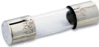
Fuse, Cartridge, Fast Acting, 5 A, 125 V, 5mm x 15mm, 0.2" x 0.59", 225 Series
- Manufacturer: LITTELFUSE
- Product type: Cartridge Fuses
- SVHC: To Be Advised
- Fuse Current: 5A
- Product Range: 225 Series
- Fuse Size Metric: 5mm x 15mm
- Fuse Size Imperial: 0.2" x 0.59"
- Voltage Rating VAC: 125V
- Blow Characteristic: Fast Acting
- Breaking Capacity Current AC: 500A
| Delivery and price | |
|---|---|
| Units per pack | 100 |
| Price | 0.411 € |
| Current stock | 50+ |
| Lead time | 30 days |
## _**WIRELESS COMMUNICATIONS DIVISION**_

**==> picture [206 x 149] intentionally omitted <==**

**----- Start of picture text -----**<br>
V V<br>CC1 CC2<br>RFIN GND<br>GND Match Match RFOUT<br>= | I]<br>VCTRL Bias Control GND<br>VREF ep LH GND<br>**----- End of picture text -----**<br>


## **TQM7638**

## _**DATA SHEET**_

_**3V HBT SiGe PCS Band CDMA 4x4mm POWER AMPLIFIER MODULE**_

## _**Features**_

## _**Product Description:**_

_The TQM7638 is a 3V, 3 stage SiGe HBT Power Amplifier Module designed for use in mobile phones.  Its extremely small 4x4mm package makes it ideal for today’s extremely small data enabled phones.  Its RF performance meets the requirements for products designed to IS-95/98 standards.  The TQM7638 provides the capability to be operated in one, two, or continuous quiescent current modes.  In digital quiescent current mode operation, the TQM7638 is controlled from the base-band processor using a CMOS compatible ICQ control voltage.  Overall current consumption of the device is minimized by selecting the lowest ICQ state available for each power output level.  RF input and output matching is included within the module; therefore, minimal external circuitry is required._

_Analog continuous bias capability with excellen linearity over 1.9 to 3.0VDC and temperature stability over –30C to 85C_

_Excellent PAE_

- _Small 10 pin 4x4mm module_

_1xRTT Compatible_

_Industry compatible digital quiescent current state control_

- _Analog continuous bias capability_

_CMOS compatible logic input_

_The TQM7638 gives excellent RF performance with low current consumption resulting in longer talk times in portable applications.  The small 6mm square surface mount package is ideal for new generation small and light phones._

## _**Electrical Specifications:**_

|Parameter|Min|Typ|Max|Units|
|---|---|---|---|---|
|Frequency|1850||1910|MHz|
|CDMA mode Pout1||28||dBm|
|CDMA Mode Efficiency1||31||%|


_Note 1: Test Conditions CDMA Mode: VCC1=3.4VDC, VCC2=3.4VDC, VREF =2.90VDC, VCTRL=0.5VDC, Tc=25°C, Pout = 28.0dBm_

_Internally matched input and output_

_Full ESD Protection_

_Low leakage current_

## _**Applications**_

_Tri Mode CDMA phones_

_PCS Band CDMA based mobile phones_

_**1**_

_For additional information and latest specifications, see our website:_ _**www.triquint.com**_

## **- TQM7638 Preliminary Data Sheet**

## _**Absolute Maximum Ratings**_

|**Symbol**|**Parameter**|**Absolute Maximum**|**Units**|
|---|---|---|---|
|||**Value**||
|VCC1,VCC2|Power Supply Voltage, no RF Applied|-0.5 to 6.0|VDC|
||RF Applied|-0.5 to 5.0||
|VREF, VCTRL|Bias reference voltages (VREF) and bias control voltage (VCTRL).|-0.5 to 5.0|VDC|
|PDISS|Power Dissipation|2.5|W|
|TC|Case Temperature, Survival|-40 to +100|°C|
|TSTG|Storage Temperature|-40 to +150|°C|
|RFIN|DC Grounded RF input, 50ohm RF impedance|0 to 0V|VDC|
|RFOUT|DC Blocked RF output, 50 ohm RF impedance|-20V to 20V|VDC|


Note: The part may not survive all maximums applied simultaneously.

## _**CDMA Mode Electrical Characteristics[1,2,3]**_

|Parameter|Conditions|Min.|Typ/Nom|Max.|Units|
|---|---|---|---|---|---|
|RF Frequency||1850||1910|MHz|
|Pout,  ICQ-hi|VCTRL= low||28||dBm|
|Large Signal Gain, ICQ-hi|Pout = 28dBm, VCTRL= low||29||dB|
|Large Signal Gain, ICQ-low|Pout = 15dBm, VCTRL= high||26||dB|
|Gain Variation vs. Temp.|-30 to 85 °C, Pout=28dBm||+/-2.5||dB|
|Quiescent Current, ICQ-hi|VCTRL= low||124||mA|
|Quiescent Current, ICQ-low|VCTRL= high||82||mA|
|Icc|Pout = 28dBm, VCTRL= low||607||mA|
|Power Added Efficiency|Pout = 28dBm, VCTRL= low||31||%|
|Adjacent Channel Power (ACP)|Pout = 28dBm, VCTRL= low, IS-95 Standard||-49|-|dBc|
|Alternate Channel Power (ALT)|Pout = 28dBm, VCTRL= low, IS-95 Standard||-58||dBc|
|Output Power Low-Power Icq state|ACPR=-47dBc, VCTRL= high, IS-95 Standard||15||dBm|


**2**

_For additional information and latest specifications, see our website:_ _**www.triquint.com**_

**- Preliminary TQM7638 Data Sheet**

## _**CDMA Mode Electrical Characteristics[1,2,3] (cont’d)**_

|Noise Power in Rx band|Pout=28dBm, VCTRL= low, IS-95 Standard||-88||dBm/30KHz|
|---|---|---|---|---|---|
|Input VSWR|Both ICQ-hi &  ICQ-low||2:1|||
|Second Harmonic|Pout=+28dBm, VCTRL= low, IS-95 Standard|||<-35|dBc|
|Third Harmonic|Pout=+28dBm, VCTRL= low, IS-95 Standard|||<-45|dBc|
|Recommended Supply Voltage||3.2|3.4|4.2|VDC|
|Reference Voltage||2.85|2.9|2.95|VDC|
|VREFCurrent, ICQ-hi|Hi-Power Mode, VCTRL= low||14||mA|
|VREFCurrent, ICQ-low|Low-Power Mode, VCTRL= high||6||mA|
|Leakage Current|VCTRL= low, VREF=0VDC||10||µA|
|Logic Current (VCTRL)||||100|µA|
|Logic Voltage (VCTRL)|High|1.7|2.0|3.5|VDC|
||Low|0|0.25|0.5|VDC|
|Recommended Operating Temperature||-30||+85C||
|Ruggedness|No Damage, Pout=+28dBm, VCTRL= low, IS-95|||10:1||
||Standard|||||
|Stability|No Oscillations, Pout=+28dBm, VCTRL= low, IS-|||10:1||
||95 Standard|||||


_**Note 1:** Test Conditions:  VCC1=3.4VDC, VCC2=3.4VDC, VREF=2.90VDC, VCTRL=0.5VDC, RF=1880MHz, TC = 25_ ° _C unless otherwise specified._ _**Note 2** : Min./Max. limits are at +25_ ° _C case temperature unless otherwise specified._ _**Note 3** : TriQuint Test Board._

**3**

_For additional information and latest specifications, see our website:_ _**www.triquint.com**_

**- TQM7638 Preliminary Data Sheet**

## **Application/Test Circuit:**

**==> picture [319 x 292] intentionally omitted <==**

**----- Start of picture text -----**<br>
C1 VCC1 V C2<br>HE V CC2 Lj}<br>REF<br>IE h<br>}— 1<br>C3<br>C4<br>V V<br>CC1 CC2<br>RFin<br>GND<br>© RFIN<br>RFout<br>a TQM7638RF<br>J1 , GND OUT 6) J2<br>V<br>CTRL VCTRL GND oF<br>C5<br>V GND<br>REF<br>t<br>4<br>C6 | VREF |<br>**----- End of picture text -----**<br>


## _**U.S. PCS Band, 1850 - 1910 MHz**_

## _**Bill of Material for TQM7638 Power Amplifier Module Application/Test Circuit***_

|Component|Reference<br>Designator|Part<br>Number|Value,<br>Cellular Band|Size|
|---|---|---|---|---|
|Power Amplifier Module||TQM7638||8pin/6mmsquare|
|RF Connector|J1, J2||||
|Capacitor|C3||100pF|0402|
|Capacitor|C3,C4,C5,C6||0.1µF|0402|
|Capacitor|C1,C2||10µF|1210|


*May vary due to printed circuit board layout and material

**4** _For additional information and latest specifications, see our website:_ _**www.triquint.com**_

**- Preliminary TQM7638 Data Sheet**

## _**Product Description:**_

The TQM7638 is a three stage SiGe HBT power amplifier module in a cascade configuration intended for use in CDMA PCS band transmit paths.

## _**Operation**_

The operation modes of the TQM7638 are determined based on the setting of VCNTRL and VREF.  The truth table below defines the operating mode.  Also, If the TQM7638 will be used in continuous bias mode VCNTRL must be connected on the circuit board to ground.

|Operating<br>Mode|VCNTRL|VREF|
|---|---|---|
|High Power|Low|>2.7VDC|
|Low-Power|High|>2.7VDC|
|Continuous<br>Bias|Gnd|~1.9 to<br>3.0VDC|
|Off|Low|0VDC|


## _**Application**_

The applications circuit for the TQM7638 is very simple since most of the critical components are included inside the module. There are several important considerations when using the module in a phone design.

First of all, it is important that the source impedance of the VCC power supply be very low. This is because the high current demand during the modulation peaks of the CDMA waveform can introduce voltage ripple at the symbol rate that will introduce additional inter-modulation distortion or Adjacent Channel Power distortion at the output of the power amplifier. If the power amplifier has a quiescent current of 100 mA and a peak current demand in excess of 1 amp, it is possible to see 900 mA change in the current required from VCC as the modulated signal moves from one extreme to the other.  If the power supply source

impedance were 1 ohm, the resulting voltage ripple would be 0.9 volts which would cause the amplifier to fail it ACP requirements. Generally, the power supply source impedance should be kept as low as possible, preferably below 0.1 ohms total.  Most battery technologies used in cellular telephones will support a low source impedance, but it may be necessary to supplement this in some designs with an low ESR capacitor.  Ceramic or tantalum capacitors of approximately 10 micro-farads work well for this requirement.

The application circuit includes 0.1 µF capacitors at the PA control line and VCC lines to ensure proper RF bypassing.  Depending on the phone board layout and circuit bypassing in other areas of the phone, some of these components may not be necessary.  There are a number of VCO signals and IF signals used in a given phone design, so it is important to protect the PA module from interfering signals and to limit any interference coming from the PA itself.  Care should be taken when removing any of the RF bypassing components.

One final area of concern is with excessive bypassing.  If too large a value of bypassing capacitor is used on the control line, it could reduce the frequency response of the control line to the point where a specification failure could occur.  Please be sure that the logic line and regulated supply lines driving the power amplifier control lines are adequate to supply peak current requirements of the bypassing capacitors chosen on the control lines.

## _**One Bias State Operation**_

The TQM7638 can be operated using one bias state.  If this mode is selected, VCNTRL should be connected to ground.

## _**Continuous Bias State Operation**_

The TQM7638 can be operated in continuous bias mode in which the VREF voltage is varied from ~1.9V to 3.0V to set the PAM quiescent current as appropriate for the desired output power level.  In this mode, VCNTRL should be connected to ground on the phone board.  Specific application circuit information for this mode is available upon request.

**5**

_For additional information and latest specifications, see our website:_ _**www.triquint.com**_

## **- TQM7638 Preliminary Data Sheet**

## _**Package Pin-Out:**_

**==> picture [271 x 227] intentionally omitted <==**

**----- Start of picture text -----**<br>
1 10<br>V V<br>CC1 CC2<br>2 GND 9<br>RF<br>IN RF<br>OUT<br>3 Match Match 8<br>a n =<br>GND<br>GND<br>4 Bias Control 7<br>V<br>CTRL<br>V<br>o REF t<br>GND<br>5 6<br>**----- End of picture text -----**<br>


## _**Pin Descriptions:**_

|**Pin Name**|**Pin #**<br>~~||~~|**Description and Usage (Equivalent Circuit)**|
|---|---|---|
|GND|Paddle<br>~~||~~<br>~~||~~|Device Ground and Heat Sink.  Needs good thermal path to remove heat.|
|VCC1|1<br>~~_~~|Collector supply for input stage.|
|RFin|2<br>7|RF input.  The RF circuit is DC grounded.  50 Ohm RF<br>impedance.<br>**RFin**<br>-|
|VCTRL|4<br>~~_~~|CMOS compatible logic level to set bias level|
|VREF|5<br>~~|~~|Regulated supply for setting bias.  Vref is set to 0VDC to power-off the TQM7638|
|RFOUT|8<br>~~_~~|RF output.  The RF circuit is DC blocked internally.  50 ohm RF impedance.|
|VCC2|10<br>~~||~~|Collector supply for output stage.|
|GND|3, 6, 7, 9<br>~~|~~|Ground|


TriQuint recommends use of several via holes to the backside ground under the Paddle.

**6**

_For additional information and latest specifications, see our website:_ _**www.triquint.com**_

**- Preliminary TQM7638 Data Sheet**

## _**Recommended PC board layout to Accept 10 Pin Module Package:**_

||||||||**J**|||||**T**|**T**|**U**|||||||||
|---|---|---|---|---|---|---|---|---|---|---|---|---|---|---|---|---|---|---|---|---|---|---|
||||||||||||||||||||||||
||||||||||||||||||||||||
|||**K**|||||||||||||||||||||
||||||||||||||||||||||||
||||||||||||||||||||||||
||||||||||||||||||||||||
|**D**||**M**<br>**N**<br>**S**<br>mil|||||||||||||||||||||
||||||||||||||||||||||||
|||||||||||||**E**|||||||||||
||||||||||||||||||||||||
||||||||**DIMENSION**|||||||**MM**|||||||||
||||||||||**D**|||||3.85|||||||||
||||||||||**E**|||||4.30|||||||||
||||||||||**J**|||||0.68|||||||||
|||||||||**K**||||||0.45|||||||||
|||||||||**M**||||||0.85|||||||||
||||||||||**N**|||||1.90|||||||||
||||||||||**S**|||||3.80|||||||||
||||||||||**T**|||||2.00|||||||||
||||||||||**U**|||||1.00|||||||||


Notes:

> 1 Only ground signal traces are allowed directly under the package

> 2 Primary dimensions are in millimeters alternate dimensions are in inches.

**7**

_For additional information and latest specifications, see our website:_ _**www.triquint.com**_

## **- TQM7638 Preliminary Data Sheet**

## _**Package Type: 10 Pin Plastic Module Package**_

**==> picture [179 x 124] intentionally omitted <==**

**----- Start of picture text -----**<br>
Pin 1<br>10<br>Pin 1<br>9<br>2<br>Indicator<br>3 8<br>4 7<br>5 6<br>**----- End of picture text -----**<br>


_**Top View**_

_**Side View**_

**==> picture [126 x 125] intentionally omitted <==**

**----- Start of picture text -----**<br>
5 6<br>4 ! 7<br>3 8<br>2 9<br>1 10<br>**----- End of picture text -----**<br>


_**Bottom View**_

**8**

_For additional information and latest specifications, see our website:_ _**www.triquint.com**_

**- Preliminary TQM7638 Data Sheet**

## _**Package Type:  10 Pin Plastic Module Package (cont’d)**_

|**DESIGNATION**|**DESCRIPTION**|**DIMENSION**|
|---|---|---|
|A|OVERALL HEIGHT|1.06<br>+/-0.09 mm|
|D|PACKAGE LENGTH|4.0 +/-0.1 mm|
|E|PACKAGE WIDTH|4.0 +/-0.1 mm|
|J|SOLDER MASK OPENING LENGTH AND WIDTH|0.575 +/-0.075 mm|
|K|METAL PAD LENGTH AND WIDTH|0.40 +/-0.05 mm|
|P|DISTANCE BETWEEN METAL PAD AND PACKAGE<br>EDGE|0.10 +/-0.025 mm|
|T|GND SOLDER MASK  OPENING WIDTH|2.00 +/-0.05 mm|
|S|GND SOLDER MASK  OPENING LENGTH|3.80 +/-0.05 mm|
|R|DISTANCE BETWEEN GND SOLDER MASK OPENING<br>AND PACKAGE EDGE|0.10 +/-0.1 mm|
|Q|DISTANCE BETWEEN GND SOLDER MASK OPENING<br>AND PACKAGE EDGE|1.00 +/-0.1 mm|
|e|TERMINAL PITCH FOR TERMINAL 1-10, 2-9, 3-8, 4-7<br>AND 5-6|3.400 mm|
|e1|TERMINAL PITCH FOR TERMINAL 1-2-3-4-5 AND 6-7-<br>8-9-10|0.850 mm|


Notes:

## _**1. GND SOLDER MASK OPENING IS NOT CENTERED ON THE PACKAGE**_

## _**Additional Information**_

For latest specifications, additional product information, worldwide sales and distribution locations, and information about TriQuint:

**Web: www.triquint.com Tel:  (503) 615-9000 Email: info_wireless@tqs.com Fax: (503) 615-8902**

For technical questions and additional information on specific applications:

## **Email: info_wireless@tqs.com**

The information provided herein is believed to be reliable; TriQuint assumes no liability for inaccuracies or omissions. TriQuint assumes no responsibility for the use of this information, and all such information shall be entirely at the user's own risk. Prices and specifications are subject to change without notice. No patent rights or licenses to any of the circuits described herein are implied or granted to any third party.

TriQuint does not authorize or warrant any TriQuint product for use in life-support devices and/or systems.

Copyright © 2002 TriQuint Semiconductor, Inc.  All rights reserved.

## Revision 0.4, September 24, 2002

_For additional information and latest specifications, see our website:_ _**www.triquint.com**_ **9**
Updated at June 4, 2026
Founded in 1927 and headquartered in Chicago, Illinois, Littelfuse is a premier global manufacturer of circuit protection, power control, and sensing technologies. Widely recognized for pioneering the first small, fast-acting protective fuse, the company has grown into an industry leader whose highly reliable components are essential to modern industrial, transportation, and consumer electronics applications worldwide. At the core of the Littelfuse portfolio is an expansive and industry-leading range of circuit protection solutions. This encompasses a massive selection of traditional fuses, fuse holders, and resettable PTC thermistor fuses designed to safely interrupt overcurrent conditions. To defend against electrical overstress, Littelfuse also provides advanced transient voltage suppression (TVS) technologies, including thousands of specialized TVS diodes, TVS varistors, and gas discharge tubes (GDTs) that ensure robust defense against voltage spikes and environmental hazards. Beyond its foundational protection components, Littelfuse manufactures a diverse array of discrete semiconductors, sensors, and switching devices. Engineers rely on their high-performance thyristors, including TRIACs and SCRs, alongside power-efficient Schottky diodes and MOSFETs for demanding power control applications. Complemented by precision proximity sensors and highly reliable reed and solid-state relays, Littelfuse delivers the critical building blocks required for secure, efficient, and complete system design.
About Novapart
Novapart is a B2B electronic component broker specialising in stock shortages and cost reduction. We source hard-to-find parts and identify compliant alternatives across a catalogue of 540,000+ components from 500+ manufacturers.
Learn more →Stock Shortage Specialist
When a component is unavailable, discontinued or has an unacceptable lead time, we tap into our network of vetted European and Asian distributors to source what you need — without compromising on quality or traceability.
Request a quote →Compliant Alternatives
We identify pin-to-pin, electrically equivalent substitutes that meet the same certifications (RoHS, AEC-Q100, REACH) as your original specification — validated against datasheets, not just part numbers. Often at a lower cost.
BOM Analysis service →