


02 04 160 1101
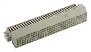
Connector, DIN41612, har-bus 64, 160 Contacts, 2.54 mm, Receptacle, Through Hole, 5 Rows
- Manufacturer: HARTING
- Product type:
- Product Range:har-bus 64 Series; No. of Contacts:160Contacts; Card Edge / Backplane Connector Type:Backplane; Pitch Spacing:2.54mm; Gender:Receptacle; Contact Termination Type:Through Hole; No.
- SVHC: No SVHC (25-Jun-2025)
- Gender: Receptacle
- Row Pitch: 2.54mm
- No. of Rows: 5Rows
- Pitch Spacing: 2.54mm
- Product Range: har-bus 64
- Contact Plating: Gold Plated Contacts
- No. of Contacts: 160Contacts
- Contact Material: -
- Contact Termination Type: Through Hole
- Card Edge / Backplane Connector Type: Backplane
| Delivery and price | |
|---|---|
| Units per pack | 25 |
| Price | 57.09 € |
| Current stock | 50+ |
| Lead time | 30 days |
|aeaeQC<br>'<br>RoHS<br>Soldering instructions<br>wamnng = QIN Signal har-bus 64 female angled TC <> cM|e<br>The connectors should be protected when being soldered<br>contaminated as a result of soldering operations or deformed<br>Generalinformation<br>(1) For prototypes and short runs protect the connectors<br>Cover the underside of the connector moulding and the <br>Design<br>IEC 61076-4-113<br>type: har-bus 64 transition connector<br>will prevent heat and gases of the soldering apparatus <br>No, of contacts<br>max. 160<br>suffice.<br>Lonfact spacing Sm<br>(2) For large series a jig is recommended. Its protective <br>Test voltage<br>1000V<br>from gas and heat generated by the soldering apparatus.<br>Contact resistance<br>max, 20m0hm<br>that should not be soldered.<br>Insulation resistance<br>min. 10°0hm<br>Working current<br>1A at 70°C (see derating diagram)<br>Cross section of solder pins<br>Temperature range<br>-55°C<br>.. +125°C<br>Termination technology<br>solder pins<br>Recommended plated hole diameter: @ 1+ 0,1mm<br>Clearance & creepaae<br>0.6mm between the rows<br>pag<br>0.8mm between two contacts in a row<br>Row z,a: A= 0,18mm? - 0,21mm?<br>Row<br>b, c, d: A= 0,19mm?<br>Insertion and withdrawal force<br>max. 160N<br>103<br>PCB thickness<br>min. 1,6mm<br>0,76%<br>0,850,<br>Mating cycles<br>PL<br>1 acc. to IEC 61076-4-113<br>500 mating cycles<br>UL<br>file<br>E102079<br>_<br>C | RoHS - compliant<br>Yes<br>@<br>Leadfree<br>Yes<br>S|<br>Insulator material<br>Material<br>PBT (thermoplastics, glass fibre reinforcement 30%)<br>Colour<br>RAL 7032 (grey)<br>UL classification<br>UL 94-V0<br>Material group acc. to IEC 60664-1<br>lila (175 < CTI < 400)<br>NF classification<br>13, F4<br>Contact material<br>Contact material<br>Copper alloy<br>Plating termination zone<br>Sn over Ni<br>Plating contact zone<br>Au over Ni<br>Derating diagram acc. to IEC 60512-5 (Current carrying capacity)<br>The current carrying capacity is limited by maximum temperature<br>E | of materials for inserts and contacts including terminals.<br>2,0<br>The current capacity curve is valid for continuous, non<br>=<br>interrupted current loaded contacts of connectors when<br>~<br>«S<br>simultaneous power on all contacts is given, without exceeding<br>°<br>the maximum temperature.<br>=<br>Control and test procedures according to DIN IEC 60512-5<br>gs<br>10<br>With selective loading higher currents can be transmitted. The<br>a 05<br>Ej@- Original Size DIN A3<br>1<br>requirements according to VITA 1.? are fulfilled.<br>All rights reserved<br>Created by<br>Inspected<br>seuinnl<br>TADJE<br>ZWAHR<br>0,0<br>“perme<br>EC PD - DE<br>ri<br>rr<br>a<br>a<br>"= DN Signal har-bus<br>Temperature [°C]<br>HARTING Electronics GmbH<br>Type<br>Number<br>388phan<br>a<br>a<br>a<br>GeSD<br>COSO|aeaeQC<br>'<br>RoHS<br>Soldering instructions<br>wamnng = QIN Signal har-bus 64 female angled TC <> cM|e<br>The connectors should be protected when being soldered<br>contaminated as a result of soldering operations or deformed<br>Generalinformation<br>(1) For prototypes and short runs protect the connectors<br>Cover the underside of the connector moulding and the <br>Design<br>IEC 61076-4-113<br>type: har-bus 64 transition connector<br>will prevent heat and gases of the soldering apparatus <br>No, of contacts<br>max. 160<br>suffice.<br>Lonfact spacing Sm<br>(2) For large series a jig is recommended. Its protective <br>Test voltage<br>1000V<br>from gas and heat generated by the soldering apparatus.<br>Contact resistance<br>max, 20m0hm<br>that should not be soldered.<br>Insulation resistance<br>min. 10°0hm<br>Working current<br>1A at 70°C (see derating diagram)<br>Cross section of solder pins<br>Temperature range<br>-55°C<br>.. +125°C<br>Termination technology<br>solder pins<br>Recommended plated hole diameter: @ 1+ 0,1mm<br>Clearance & creepaae<br>0.6mm between the rows<br>pag<br>0.8mm between two contacts in a row<br>Row z,a: A= 0,18mm? - 0,21mm?<br>Row<br>b, c, d: A= 0,19mm?<br>Insertion and withdrawal force<br>max. 160N<br>103<br>PCB thickness<br>min. 1,6mm<br>0,76%<br>0,850,<br>Mating cycles<br>PL<br>1 acc. to IEC 61076-4-113<br>500 mating cycles<br>UL<br>file<br>E102079<br>_<br>C | RoHS - compliant<br>Yes<br>@<br>Leadfree<br>Yes<br>S|<br>Insulator material<br>Material<br>PBT (thermoplastics, glass fibre reinforcement 30%)<br>Colour<br>RAL 7032 (grey)<br>UL classification<br>UL 94-V0<br>Material group acc. to IEC 60664-1<br>lila (175 < CTI < 400)<br>NF classification<br>13, F4<br>Contact material<br>Contact material<br>Copper alloy<br>Plating termination zone<br>Sn over Ni<br>Plating contact zone<br>Au over Ni<br>Derating diagram acc. to IEC 60512-5 (Current carrying capacity)<br>The current carrying capacity is limited by maximum temperature<br>E | of materials for inserts and contacts including terminals.<br>2,0<br>The current capacity curve is valid for continuous, non<br>=<br>interrupted current loaded contacts of connectors when<br>~<br>«S<br>simultaneous power on all contacts is given, without exceeding<br>°<br>the maximum temperature.<br>=<br>Control and test procedures according to DIN IEC 60512-5<br>gs<br>10<br>With selective loading higher currents can be transmitted. The<br>a 05<br>Ej@- Original Size DIN A3<br>1<br>requirements according to VITA 1.? are fulfilled.<br>All rights reserved<br>Created by<br>Inspected<br>seuinnl<br>TADJE<br>ZWAHR<br>0,0<br>“perme<br>EC PD - DE<br>ri<br>rr<br>a<br>a<br>"= DN Signal har-bus<br>Temperature [°C]<br>HARTING Electronics GmbH<br>Type<br>Number<br>388phan<br>a<br>a<br>a<br>GeSD<br>COSO|aeaeQC|QC|QC|QC<br>QO<br>soldered in a dip, flow or film soldering bath. Otherwise, they might become<br>deformed as a result of overheating.<br>connectors with an industrial adhesive tape, e.g. Tesaband 4331 (www.tesa.de),<br> adjacent parts of the pcb as well as the open sides of the connector. This<br> from damaging the connector. About 140 + 5 mm of the tape should<br> cover with a fast action mechanical locking device shields the connectors<br>apparatus. As an additional protection a foil can be used for covering the parts<br>0,19mm? - 0,22mm?<br>_<br>g<br>C<br>S<br>E|QC<br>QO<br>soldered in a dip, flow or film soldering bath. Otherwise, they might become<br>deformed as a result of overheating.<br>connectors with an industrial adhesive tape, e.g. Tesaband 4331 (www.tesa.de),<br> adjacent parts of the pcb as well as the open sides of the connector. This<br> from damaging the connector. About 140 + 5 mm of the tape should<br> cover with a fast action mechanical locking device shields the connectors<br>apparatus. As an additional protection a foil can be used for covering the parts<br>0,19mm? - 0,22mm?<br>_<br>g<br>C<br>S<br>E|
|---|---|---|---|---|---|---|
||aeae<br>'<br>RoHS<br>Soldering instructions<br>wamnng = QIN Signal har-bus 64 female angled TC <> cM|e<br>The connectors should be protected when being soldered<br>contaminated as a result of soldering operations or deformed<br>Generalinformation<br>(1) For prototypes and short runs protect the connectors<br>Cover the underside of the connector moulding and the <br>Design<br>IEC 61076-4-113<br>type: har-bus 64 transition connector<br>will prevent heat and gases of the soldering apparatus <br>No, of contacts<br>max. 160<br>suffice.<br>Lonfact spacing Sm<br>(2) For large series a jig is recommended. Its protective <br>Test voltage<br>1000V<br>from gas and heat generated by the soldering apparatus.<br>Contact resistance<br>max, 20m0hm<br>that should not be soldered.<br>Insulation resistance<br>min. 10°0hm<br>Working current<br>1A at 70°C (see derating diagram)<br>Cross section of solder pins<br>Temperature range<br>-55°C<br>.. +125°C<br>Termination technology<br>solder pins<br>Recommended plated hole diameter: @ 1+ 0,1mm<br>Clearance & creepaae<br>0.6mm between the rows<br>pag<br>0.8mm between two contacts in a row<br>Row z,a: A= 0,18mm? - 0,21mm?<br>Row<br>b, c, d: A= 0,19mm?<br>Insertion and withdrawal force<br>max. 160N<br>103<br>PCB thickness<br>min. 1,6mm<br>0,76%<br>0,850,<br>Mating cycles<br>PL<br>1 acc. to IEC 61076-4-113<br>500 mating cycles<br>UL<br>file<br>E102079<br>_<br>| RoHS - compliant<br>Yes<br>@<br>Leadfree<br>Yes<br>S|<br>Insulator material<br>Material<br>PBT (thermoplastics, glass fibre reinforcement 30%)<br>Colour<br>RAL 7032 (grey)<br>UL classification<br>UL 94-V0<br>Material group acc. to IEC 60664-1<br>lila (175 < CTI < 400)<br>NF classification<br>13, F4<br>Contact material<br>Contact material<br>Copper alloy<br>Plating termination zone<br>Sn over Ni<br>Plating contact zone<br>Au over Ni<br>Derating diagram acc. to IEC 60512-5 (Current carrying capacity)<br>The current carrying capacity is limited by maximum temperature<br>| of materials for inserts and contacts including terminals.<br>2,0<br>The current capacity curve is valid for continuous, non<br>=<br>interrupted current loaded contacts of connectors when<br>~<br>«S<br>simultaneous power on all contacts is given, without exceeding<br>°<br>the maximum temperature.<br>=<br>Control and test procedures according to DIN IEC 60512-5<br>gs<br>10<br>With selective loading higher currents can be transmitted. The<br>a 05<br>Ej@- Original Size DIN A3<br>1<br>requirements according to VITA 1.? are fulfilled.<br>All rights reserved<br>Created by<br>Inspected<br>seuinnl<br>TADJE<br>ZWAHR<br>0,0<br>“perme<br>EC PD - DE<br>ri<br>rr<br>a<br>a<br>"= DN Signal har-bus<br>Temperature [°C]<br>HARTING Electronics GmbH<br>Type<br>Number<br>388phan<br>a<br>a<br>a<br>GeSD<br>COSO||||QO<br>soldered in a dip, flow or film soldering bath. Otherwise, they might become<br>deformed as a result of overheating.<br>connectors with an industrial adhesive tape, e.g. Tesaband 4331 (www.tesa.de),<br> adjacent parts of the pcb as well as the open sides of the connector. This<br> from damaging the connector. About 140 + 5 mm of the tape should<br> cover with a fast action mechanical locking device shields the connectors<br>apparatus. As an additional protection a foil can be used for covering the parts<br>0,19mm? - 0,22mm?<br>_<br>g<br>S||
||||||||
|||||||C|
||||||||
|||||||E|
||||||||
||||||Inspected by<br>Standardisation<br>Date<br>State<br>ZWAHR<br>HOFFMANN<br>2013-12-04<br>Final Release||
||||||Doc-Key / ECM-Nr.<br>har-bus 64 fenale angled<br>xe||
||||||xe<br>Rev,<br>Page<br>0204220020<br>SO||
|||a<br>a<br>a<br>Ge|GeSD|COSO|||


(1) For prototypes and short runs protect the connectors with an industrial adhesive tape, e.g. Tesaband 4331 (www.tesa.de), Cover the underside of the connector moulding and the adjacent parts of the pcb as well as the open sides of the connector. This will prevent heat and gases of the soldering apparatus from damaging the connector. About 140 + 5 mm of the tape should suffice. (2) For large series a jig is recommended. Its protective cover with a fast action mechanical locking device shields the connectors from gas and heat generated by the soldering apparatus. As an additional protection a foil can be used for covering the parts that should not be soldered.

**==> picture [1121 x 568] intentionally omitted <==**

**----- Start of picture text -----**<br>
pag 0.8mm between two contacts in a row Row z,a: A= 0,18mm? - 0,21mm? Row b, c, d: A= 0,19mm? - 0,22mm?<br>Insertion and withdrawal force max. 160N<br>PCB thickness min. 1,6mm 0, 76%103 0,850,<br>Mating cycles PL 1 acc. to IEC 61076-4-113 500 mating cycles<br>UL file E102079<br>RoHS - compliant Yes @_ g_ C<br>Leadfree Yes S| S<br>Insulator material<br>Material PBT (thermoplastics, glass fibre reinforcement 30%)<br>Colour RAL 7032 (grey)<br>UL classification UL 94-V0<br>Material group acc. to IEC 60664-1 lila (175 < CTI < 400)<br>NF classification 13, F4<br>Contact material<br>Contact material Copper alloy<br>Plating termination zone Sn over Ni<br>Plating contact zone Au over Ni<br>Derating diagram acc. to IEC 60512-5 (Current carrying capacity)<br>The current carrying capacity is limited by maximum temperature<br>of materials for inserts and contacts including terminals. 2,0 E<br>The current capacity curve is valid for continuous, non =<br>interrupted current loaded contacts of connectors when ~ «S<br>simultaneous power on all contacts is given, without exceeding °<br>the maximum temperature. =<br>Control and test procedures according to DIN IEC 60512-5 gs 10<br>With selective loading higher currents can be transmitted. The a 05 Ej@- Original Size DIN A3 1<br>requirements according to VITA 1.? are fulfilled. All rights reserved Created by Inspected by Standardisation Date State<br>TADJE ZWAHR HOFFMANN 2013-12-04 Final Release<br>0,0 seuinnl“perme EC PD - DE ri Doc-Key / ECM-Nr.<br>rr a a<br>"= DN Signal har-bus 64 fenale angled<br>Temperature [°C] HARTING Electronics GmbH xe<br>Type Number Rev, Page<br>388 phan 0204220020<br>a a a Ge SD CO SO A3<br>**----- End of picture text -----**<br>


The current carrying capacity is limited by maximum temperature E | of materials for inserts and contacts including terminals.
Updated at June 7, 2026
Harting is a globally recognized leader in electrical, electronic, and optical connection, transmission, and networking technologies. Renowned for its expertise in manufacturing mechatronics and customized connectivity solutions, the company develops highly reliable products tailored for demanding applications in factory automation, rail technology, mechanical engineering, and energy distribution. Our primary selection of Harting components is centered around their robust interconnect and cabling solutions. This includes a comprehensive range of high-quality cable assemblies, featuring durable USB cables engineered for reliable data transmission. Furthermore, we offer an extensive array of terminal blocks—encompassing both pluggable and wire-to-board configurations—alongside specialized backplane connectors that guarantee secure, stable connections in complex industrial systems. Beyond their industry-leading connectors and cable assemblies, Harting's innovative engineering also extends to industrial sensing and data storage. Our portfolio features their precision current sensors and industrial-grade flash memory cards, providing a complete suite of components built to withstand the rigors of modern electronic and industrial environments.
About Novapart
Novapart is a B2B electronic component broker specialising in stock shortages and cost reduction. We source hard-to-find parts and identify compliant alternatives across a catalogue of 410,000+ components from 500+ manufacturers.
Learn more →Stock Shortage Specialist
When a component is unavailable, discontinued or has an unacceptable lead time, we tap into our network of vetted European and Asian distributors to source what you need — without compromising on quality or traceability.
Request a quote →Compliant Alternatives
We identify pin-to-pin, electrically equivalent substitutes that meet the same certifications (RoHS, AEC-Q100, REACH) as your original specification — validated against datasheets, not just part numbers. Often at a lower cost.
BOM Analysis service →