


RBA200N15YAPF-6UA03#KB0
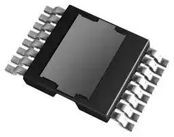
Power MOSFET, N Channel, 150 V, 200 A, 0.0034 ohm, TOLT, Surface Mount
- Manufacturer: RENESAS
- Product type:
- SVHC: No SVHC (25-Jun-2025)
- No. of Pins: 16Pins
- Channel Type: N Channel
- Product Range: REXFET-1 Series
- Qualification: AEC-Q101
- Power Dissipation: 366W
- Transistor Mounting: Surface Mount
- Rds(on) Test Voltage: 10V
- Transistor Case Style: TOLT
- Drain Source Voltage Vds: 150V
- Operating Temperature Max: 175°C
- Continuous Drain Current Id: 200A
- Drain Source On State Resistance: 0.0034ohm
- Gate Source Threshold Voltage Max: 3.7V
| Delivery and price | |
|---|---|
| Units per pack | 250 |
| Price | 3.58 € |
| Current stock | 1000+ |
| Lead time | 30 days |
Datasheet ## **RBA200N15YAPF-6UA03** ## REXFET-1 N-Channel Power MOSFET 150 V - 200 A - 3.4 mΩ - TOLT for Automotive ## **Description** The RBA200N15YAPF-6UA03 N-channel power MOSFET features REXFET-1 split-gate technology and is offered in a TOLT package. The TOLT package features top-side cooling for ultra-compact and optimal thermal performance. Renesas' REXFET-1 split gate technology is suitable for applications requiring low RDS(on) and switching capability for high-power and high-frequency applications. ## **Features** - Standard level gate drive voltage: VGS(th) = 2.2 to 3.7 V - Super low on-state resistance: RDS(on) = 3.4 m MAX. - Low input capacitance - Low thermal resistance - 100% Avalanche tested - AEC-Q101 qualified - PPAP capable - Pb-free lead plating: RoHS compliant - MSL1 classified according to IPC/JEDEC J-STD-020 ## **Application** Small Traction (2-wheel, 3-wheel vehicle), 72 to 96 V load, Onboard charger, Charging station, Low voltage DC/DC, **Outline** **==> picture [435 x 112] intentionally omitted <==** **----- Start of picture text -----**<br> 9 Drain<br>9 to 16,Heatsink<br>A200N15<br>16<br>16 Heatsink<br>8 9 Gate YUA Trace code<br>0 8<br>1 1 ag ARG<br>Source Mark part number Lot number<br>BS « 1 to 7<br>8<br>TOLT Equivalent circuit Marking Specification<br>**----- End of picture text -----**<br> ## **Absolute Maximum Ratings** (Tj = 25 °C unless otherwise notice) |**Item**|**Symbol**|**Ratings **|**Unit**| |---|---|---|---| |Drain to Source Voltage|VDSS|150|V| |Gate to Source Voltage|VGSS|±20|V| |Continuous Drain Current|ID(Tc=25°C)<br>Note 2,6|±200|A| ||ID(Tc=100°C)<br>Note 2,6|±148|A| |Pulsed Drain Current|ID(pulse)<br>Note 1,2,3,6|±800|A| |Power Dissipation|PDNote 1,6|366|W| |Operating and Storage Temperature|Tj,Tstg|-55 to 175|°C| |Single Avalanche Current|IAS<br>Note 4|75|A| |Single Avalanche Energy|EAS<br>Note 4|421|mJ| R07DS1629EJ0100 Rev.1.00 Aug.19.2025 Page 1 of 9 RBA200N15YAPF-6UA03 ## **Thermal Resistance** |**Thermal Resistance**|||||| |---|---|---|---|---|---| |**Item**|**Symbol**|**Min**|**Typ**|**Max**|**Unit**| |Junction to Case Thermal Resistance|Rth(j-c)<br>Note 6|—|—|0.41|°C/W| |Junction to Ambient Thermal Resistance|Rth(j-a)Note 5,6|—|—|40|°C/W| ## **Electrical Characteristics** (Tj = 25 °C unless otherwise notice) |**Item**|**Symbol**|**Min**|**Typ**|**Max**|**Unit**|**Test Conditions**| |---|---|---|---|---|---|---| |Zero Gate Voltage Drain Current|IDSS|—|—|1|A|VDS= 150 V, VGS= 0 V| |Gate Leakage Current|IGSS|—|—|±100|nA|VGS= ±20 V, VDS= 0 V| |Gate to Source Threshold Voltage|VGS(th)|2.2|—|3.7|V|VDS= VGS, ID= 250A| |Drain to Source On-state Resistance|RDS(on)|—|2.8|3.4|m|VGS= 10 V, ID= 100 A| |Input Capacitance|Ciss|—|6200|—|pF|VDS= 75 V, VGS= 0 V<br>f = 100 kHz| |Output Capacitance|Coss|—|2100|—|pF|| |Reverse Transfer Capacitance|Crss|—|37|—|pF|| |Gate resistance|Rg|—|4.4|—||—| |Turn-on Delay Time|td(on)|—|30|—|ns|VDD= 75 V, ID= 50 A<br>VGS= 10 V<br>RG= 5| |Rise Time|tr|—|20|—|ns|| |Turn-off Delay Time|td(off)|—|95|—|ns|| |Fall Time|tf|—|20|—|ns|| |Total Gate Charge|Qg|—|86|—|nC|VDD= 75 V, ID= 50 A<br>VGS= 10 V| |Gate to Source Charge|Qgs|—|30|—|nC|| |Gate to Drain Charge|Qgd|—|15|—|nC|| |Gate plateau voltage|Vplateau|—|5.0|—|V|| |Output Charge|Qoss|—|255|—|nC|VDS= 75 V, VGS= 0 V| |Body Diode Forward Voltage|VF(S-D)|—|0.87|1.5|V|IF= 100 A, VGS= 0 V| |Reverse Recovery Time|trr|—|120|—|ns|IF= 50 A, VGS= 0 V<br>di/dt= 100 A/s| |Reverse Recovery Charge|Qrr|—|400|—|nC|| Note 1. Tc = 25 °C 2. Value is limited by overall system design including PCB. 3. PW 10 s 4. L = 100 H, VDD = 50 V, RG = 25 5. Device on 40 mm x 40 mm x 1.5 mm epoxy PCB FR4. (2 oz Cu pad.) 6. Defined by design. Not subject to production test. R07DS1629EJ0100 Rev.1.00 Aug.19.2025 Page 2 of 9 RBA200N15YAPF-6UA03 ## **Typical Characteristics** DERATING FACTOR OF FORWARD BIAS SAFE OPERATING AREA **==> picture [181 x 387] intentionally omitted <==** **----- Start of picture text -----**<br> 120<br>100<br>80<br>60<br>40<br>20<br>0<br>0 25 50 75 100 125 150 175<br>TC - Case Temperature - °C<br>FORWARD BIAS SAFE OPERATING AREA<br>1000<br>100<br>10 T C = 25 °C<br>Single pulse<br>1<br>0.1<br>0.01<br>1 10 100 200<br>VDS - Drain to Source Voltage - V<br>RDS(on)limit<br>PW = 1 µs<br>PW = 10 µs<br>PW = 100 µs<br>PW = 1 ms<br>PW = 10 ms<br>DC<br> - Percentage of Rated Power - %dT<br> - Drain Current - A<br>ID<br>**----- End of picture text -----**<br> FORWARD BIAS SAFE OPERATING AREA **==> picture [179 x 196] intentionally omitted <==** **----- Start of picture text -----**<br> TRANSIENT THREMAL IMPEDANCE<br>vs. PULSE WIDTH<br>10<br>TC = 25 °C<br>1<br>0.1<br>0.01<br>0.001<br>10 µ 100 µ 1 m 10 m 100m 1<br>PW - Pulse Width - s<br>D = PW / T<br> D = 0.5<br> 0.2<br> 0.1<br> 0.05<br> 0.02<br> 0.01<br> Single pulse<br> - Tranjent Thermal Impedance -°C/W<br>th(t)<br>Z<br>**----- End of picture text -----**<br> TOTAL POWER DISSIPATION vs. CASE TEMPERATURE **==> picture [183 x 174] intentionally omitted <==** **----- Start of picture text -----**<br> 400<br>350<br>300<br>250<br>200<br>150<br>100<br>50<br>0<br>0 25 50 75 100 125 150 175<br>TC - Case Temperature - °C<br> - Total Power Dissipation - WPT<br>**----- End of picture text -----**<br> DRAIN CURRENT vs. CASE TEMPERATURE **==> picture [183 x 173] intentionally omitted <==** **----- Start of picture text -----**<br> 250<br>200<br>150<br>100<br>50<br>0<br>0 25 50 75 100 125 150 175<br>TC - Case Temperature - °C<br> - Drain Current - A<br>ID<br>**----- End of picture text -----**<br> AVALANCHE CHARACTERISTICS **==> picture [185 x 176] intentionally omitted <==** **----- Start of picture text -----**<br> 1000<br>100<br>10<br>T = 25 °C<br>1 j<br>Tj = 100 °C<br>T j = 150°C<br>0.1<br>0.1 1 10 100 1000<br>tAV - Time in Avalache - V<br> - Single Avalanche Current - A<br>IAS<br>**----- End of picture text -----**<br> R07DS1629EJ0100 Rev.1.00 Aug.19.2025 Page 3 of 9 RBA200N15YAPF-6UA03 **==> picture [179 x 620] intentionally omitted <==** **----- Start of picture text -----**<br> DRAIN CURRENT vs.<br>DRAIN TO SOURCE VOLTAGE<br>200<br>Tj = 25°C<br>150<br>100<br>VGS = 10 V<br>V GS = 8 V<br>50 VGS = 7 V<br>VGS = 6 V<br>VGS = 5 V<br>0<br>0 0.5 1 1.5 2<br>VDS - Drain to Source Voltage - V<br>DRAIN TO SOURCE ON-STATE RESISTANCE<br>vs. GATE TO SOURCE VOLTAGE<br>10<br>ID = 100 A<br>8 TJ = 175°C<br>TJ = 25°C<br>6<br>4<br>2<br>0<br>0 5 10 15 20<br>VGS - Gate to Source Voltage - V<br>FORWARD TRANSFER CHARACTERISTICS<br>200<br>Tj = 175 °C<br>Tj = 100 °C<br>150 T = 25 °C<br>j<br>Tj = -55 ° C<br>100<br>50<br>VDS = 5 V<br>0<br>1 2 3 4 5 6<br>VGS - Gate to Source Voltage - V<br> - Drain Current - A<br>ID<br> - Drain to Source On-State Resistance - mΩ<br>DS(on)<br>R<br> - Drain Current - A<br>ID<br>**----- End of picture text -----**<br> DRAIN TO SOURCE ON-STATE RESISTANCE vs. GATE TO SOURCE VOLTAGE FORWARD TRANSFER CHARACTERISTICS **==> picture [181 x 196] intentionally omitted <==** **----- Start of picture text -----**<br> DRAIN TO SOURCE ON-STATE<br>RESISTANCE vs. DRAIN CURRENT<br>10<br>T = 25°C<br>j<br>8 VGS = 5 V<br>VGS = 6 V<br>6 VGS = 7 V<br>VGS = 8 V<br>4 VGS = 10 V<br>2<br>0<br>0 50 100 150 200<br>ID - Drain Current - A<br> - Drain to Source On-State Resistance - mΩ<br>DS(on)<br>R<br>**----- End of picture text -----**<br> **==> picture [189 x 410] intentionally omitted <==** **----- Start of picture text -----**<br> DRAIN TO SOURCE ON-STATE RESISTANCE<br>vs. JUNCTION TEMPERATURE<br>10<br>8<br>6<br>4<br>2<br>V GS = 10 V<br>I D = 100 A<br>0<br>-75 -25 25 75 125 175<br>Tj - Junction Temperature -°C<br>GATE TO SOURCE THRESHOLD VOLTAGE<br>vs. JUNCTION TEMPERATURE<br>5<br>V DS = V GS<br>4 ID = 2.5 mA<br>ID = 250 µA<br>3<br>2<br>1<br>0<br>-75 -25 25 75 125 175<br>Tj - Junction Temperature -°C<br> - Drain to Source On-State Resistance - mΩ<br>DS(on)<br>R<br> - Gate to Source Thereshold Voltage - V<br>GS(th)<br>V<br>**----- End of picture text -----**<br> R07DS1629EJ0100 Rev.1.00 Aug.19.2025 Page 4 of 9 RBA200N15YAPF-6UA03 **==> picture [183 x 192] intentionally omitted <==** **----- Start of picture text -----**<br> CAPACITANCE vs.<br>DRAIN TO SOURCE VOLTAGE<br>10000<br>1000<br>C iss<br>100 Coss<br>Crss<br>V GS = 0 V<br>f = 100 kHz<br>10<br>0 50 100 150<br>VDS - Drain to Source Voltage - V<br> - Capacitance - pF<br>rss<br>C<br>oss ,<br>C<br>iss ,<br>C<br>**----- End of picture text -----**<br> SOURCE TO DRAIN DIODE FORWARD VOLTAGE **==> picture [185 x 174] intentionally omitted <==** **----- Start of picture text -----**<br> 200<br>VGS = 0 V<br>Tj = 175 °C<br>150<br>Tj = 100 °C<br>T = 25 °C<br>j<br>100 T j = -55 ° C<br>50<br>0<br>0 0.4 0.8 1.2<br>VF(S-D) - Source to Drain Forward Voltage - V<br> - Diode Forward Current - AIF<br>**----- End of picture text -----**<br> **==> picture [190 x 403] intentionally omitted <==** **----- Start of picture text -----**<br> DYNAMIC INPUT/OUTPUT CHARACTERISTICS<br>10<br>8<br>6<br>4<br>VDD = 75 V<br>2<br>ID = 50 A<br>T = 25 °C<br>j<br>0<br>0 20 40 60 80 100<br>Qg - Gate Charge - nC<br>DRAIN-SOURCE BREAKDOWN BOLTAGE<br>170<br>160<br>150<br>140<br>130<br>VGS = 0 V<br>I D = 10 mA<br>120<br>-75 -25 25 75 125 175<br>Tj - Junction Temprature -°C<br> - Gate to Source Voltage - V<br>GS<br>V<br> - Drain to Source Voltage - V<br>(BR)DSS<br>V<br>**----- End of picture text -----**<br> R07DS1629EJ0100 Rev.1.00 Aug.19.2025 Page 5 of 9 RBA200N15YAPF-6UA03 ## **Test Circuit** **==> picture [419 x 634] intentionally omitted <==** **----- Start of picture text -----**<br> Avalanche<br>Test Circuit Waveform<br>L V(BR)DSS<br>IAS<br>ID<br>VDD<br>RG VDD 0 VDS<br>D.U.T.<br>VGS<br>VGS<br>0<br>EAS = [1] 2 ・ V(BR)DSS<br>2 [・L・] [I][AS] V(BR)DSS - VDD<br>Switching Time<br>Test Circuit Waveform<br>RL<br>90%<br>VGS 10%<br>RG D.U.T. VDD VDS 90% 90%<br>1 0% 10%<br>VGS<br>td(on) tr td(off) tf<br>Gate Charge<br>Test Circuit Waveform<br>RL<br>Qg VGS<br>IG<br>D.U.T. VDD<br>Vplateau<br>VGS<br>Qgs Qgd<br>Reverse Recovery<br>Test Circuit Waveform<br>IF<br>IF<br>D.U.T.<br>L<br>trr<br>di/dt<br>RG VDD 0 Qrr<br>VGS<br>**----- End of picture text -----**<br> R07DS1629EJ0100 Rev.1.00 Aug.19.2025 Page 6 of 9 RBA200N15YAPF-6UA03 ## **Package Dimensions** **==> picture [398 x 443] intentionally omitted <==** **----- Start of picture text -----**<br> E DETAIL. A<br>E1<br>E2<br>0.20<br>e b 0.25 M c Mass : 0.85 g<br>DIMENSION (mm)<br>SYMBOL<br>MIN NOM MAX<br>A 2.20 2.30 2.35<br>A1 0.01 - 0.16<br>A3 - 0.5 -<br>b 0.60 0.70 0.85<br>c 0.45 0.50 0.65<br>D 10.00 10.10 10.30<br>D1 - 5.67 -<br>D2 - 2.00 -<br>D3 - 5.05 -<br>D4 5.00 5.05 5.13<br>E 9.70 9.90 10.10<br>E1 - 9.46 -<br>Lp E2 - 8.30 -<br>e 1.20BSC<br>DETAIL. A<br>H 14.80 15.00 15.20<br>L 2.25 2.45 2.65<br>Lp 1.30 1.50 1.70<br>D4<br>D D1 D2 H<br>D3<br>L<br>A3<br>A A1<br>**----- End of picture text -----**<br> ## **Mount pad** **==> picture [187 x 186] intentionally omitted <==** **----- Start of picture text -----**<br> 0.8 1.20<br>Unit : mm<br>2.85<br>6.925<br>6.925<br>**----- End of picture text -----**<br> R07DS1629EJ0100 Rev.1.00 Aug.19.2025 Page 7 of 9 RBA200N15YAPF-6UA03 ## **Ordering Information** |**Ordering Information**||| |---|---|---| |**Part No.**|Packing|**Quantity**| |RBA200N15YAPF-6UA03#KB0|Taping|1300pcs/reel| ## **Packing Specification** **==> picture [362 x 438] intentionally omitted <==** **----- Start of picture text -----**<br> Feed direction<br>P0 P2 P Φ D0 T<br>1pin<br>Φ D1<br>T<br>Product orientation<br>A0 Unit : mm<br>W1 Symbol Dimension<br>W 24<br>P 16<br>P0 4<br>P2 2<br>A0 10.4<br>B0 15.5<br>Tape Dimension B1 10.0<br>K0 2.65<br>F 11.5<br>E 1.75<br>D0 1.5<br>G D1 1.5<br>T 0.4<br>A 330<br>2.3 W2 Reel Dimension N 100<br>W1 25.4<br>W2 29.4<br>13.5<br>Detail.G<br>E<br>F<br>W<br>B1 B0<br>K0<br>N A<br>**----- End of picture text -----**<br> Remark: Strong electric field, when exposed to this device, can cause destruction of the gate oxide and ultimately degrade the device operation. Steps must be taken to stop generation of static electricity as much as possible, and quickly dissipate it once, when it has occurred. R07DS1629EJ0100 Rev.1.00 Aug.19.2025 Page 8 of 9 ## **Notice** 1. Descriptions of circuits, software and other related information in this document are provided only to illustrate the operation of semiconductor products and application examples. You are fully responsible for the incorporation or any other use of the circuits, software, and information in the design of your product or system. Renesas Electronics disclaims any and all liability for any losses and damages incurred by you or third parties arising from the use of these circuits, software, or information. 2. Renesas Electronics hereby expressly disclaims any warranties against and liability for infringement or any other claims involving patents, copyrights, or other intellectual property rights of third parties, by or arising from the use of Renesas Electronics products or technical information described in this document, including but not limited to, the product data, drawings, charts, programs, algorithms, and application examples. 3. No license, express, implied or otherwise, is granted hereby under any patents, copyrights or other intellectual property rights of Renesas Electronics or others. 4. You shall be responsible for determining what licenses are required from any third parties, and obtaining such licenses for the lawful import, export, manufacture, sales, utilization, distribution or other disposal of any products incorporating Renesas Electronics products, if required. 5. You shall not alter, modify, copy, or reverse engineer any Renesas Electronics product, whether in whole or in part. Renesas Electronics disclaims any and all liability for any losses or damages incurred by you or third parties arising from such alteration, modification, copying or reverse engineering. 6. Renesas Electronics products are classified according to the following two quality grades: “Standard” and “High Quality”. The intended applications for each Renesas Electronics product depends on the product’s quality grade, as indicated below. - "Standard": Computers; office equipment; communications equipment; test and measurement equipment; audio and visual equipment; home electronic appliances; machine tools; personal electronic equipment; industrial robots; etc. - "High Quality": Transportation equipment (automobiles, trains, ships, etc.); traffic control (traffic lights); large-scale communication equipment; key financial terminal systems; safety control equipment; etc. - Unless expressly designated as a high reliability product or a product for harsh environments in a Renesas Electronics data sheet or other Renesas Electronics document, Renesas Electronics products are not intended or authorized for use in products or systems that may pose a direct threat to human life or bodily injury (artificial life support devices or systems; surgical implantations; etc.), or may cause serious property damage (space system; undersea repeaters; nuclear power control systems; aircraft control systems; key plant systems; military equipment; etc.). Renesas Electronics disclaims any and all liability for any damages or losses incurred by you or any third parties arising from the use of any Renesas Electronics product that is inconsistent with any Renesas Electronics data sheet, user’s manual or other Renesas Electronics document. 7. No semiconductor product is absolutely secure. Notwithstanding any security measures or features that may be implemented in Renesas Electronics hardware or software products, Renesas Electronics shall have absolutely no liability arising out of any vulnerability or security breach, including but not limited to any unauthorized access to or use of a Renesas Electronics product or a system that uses a Renesas Electronics product. RENESAS ELECTRONICS DOES NOT WARRANT OR GUARANTEE THAT RENESAS ELECTRONICS PRODUCTS, OR ANY SYSTEMS CREATED USING RENESAS ELECTRONICS PRODUCTS WILL BE INVULNERABLE OR FREE FROM CORRUPTION, ATTACK, VIRUSES, INTERFERENCE, HACKING, DATA LOSS OR THEFT, OR OTHER SECURITY INTRUSION (“Vulnerability Issues”). RENESAS ELECTRONICS DISCLAIMS ANY AND ALL RESPONSIBILITY OR LIABILITY ARISING FROM OR RELATED TO ANY VULNERABILITY ISSUES. FURTHERMORE, TO THE EXTENT PERMITTED BY APPLICABLE LAW, RENESAS ELECTRONICS DISCLAIMS ANY AND ALL WARRANTIES, EXPRESS OR IMPLIED, WITH RESPECT TO THIS DOCUMENT AND ANY RELATED OR ACCOMPANYING SOFTWARE OR HARDWARE, INCLUDING BUT NOT LIMITED TO THE IMPLIED WARRANTIES OF MERCHANTABILITY, OR FITNESS FOR A PARTICULAR PURPOSE. 8. When using Renesas Electronics products, refer to the latest product information (data sheets, user’s manuals, application notes, “General Notes for Handling and Using Semiconductor Devices” in the reliability handbook, etc.), and ensure that usage conditions are within the ranges specified by Renesas Electronics with respect to maximum ratings, operating power supply voltage range, heat dissipation characteristics, installation, etc. Renesas Electronics disclaims any and all liability for any malfunctions, failure or accident arising out of the use of Renesas Electronics products outside of such specified ranges. 9. Although Renesas Electronics endeavors to improve the quality and reliability of Renesas Electronics products, semiconductor products have specific characteristics, such as the occurrence of failure at a certain rate and malfunctions under certain use conditions. Unless designated as a high reliability product or a product for harsh environments in a Renesas Electronics data sheet or other Renesas Electronics document, Renesas Electronics products are not subject to radiation resistance design. You are responsible for implementing safety measures to guard against the possibility of bodily injury, injury or damage caused by fire, and/or danger to the public in the event of a failure or malfunction of Renesas Electronics products, such as safety design for hardware and software, including but not limited to redundancy, fire control and malfunction prevention, appropriate treatment for aging degradation or any other appropriate measures. Because the evaluation of microcomputer software alone is very difficult and impractical, you are responsible for evaluating the safety of the final products or systems manufactured by you. 10. Please contact a Renesas Electronics sales office for details as to environmental matters such as the environmental compatibility of each Renesas Electronics product. You are responsible for carefully and sufficiently investigating applicable laws and regulations that regulate the inclusion or use of controlled substances, including without limitation, the EU RoHS Directive, and using Renesas Electronics products in compliance with all these applicable laws and regulations. Renesas Electronics disclaims any and all liability for damages or losses occurring as a result of your noncompliance with applicable laws and regulations. 11. Renesas Electronics products and technologies shall not be used for or incorporated into any products or systems whose manufacture, use, or sale is prohibited under any applicable domestic or foreign laws or regulations. You shall comply with any applicable export control laws and regulations promulgated and administered by the governments of any countries asserting jurisdiction over the parties or transactions. 12. It is the responsibility of the buyer or distributor of Renesas Electronics products, or any other party who distributes, disposes of, or otherwise sells or transfers the product to a third party, to notify such third party in advance of the contents and conditions set forth in this document. 13. This document shall not be reprinted, reproduced or duplicated in any form, in whole or in part, without prior written consent of Renesas Electronics. 14. Please contact a Renesas Electronics sales office if you have any questions regarding the information contained in this document or Renesas Electronics products. - (Note1) “Renesas Electronics” as used in this document means Renesas Electronics Corporation and also includes its directly or indirectly controlled subsidiaries. (Note2) “Renesas Electronics product(s)” means any product developed or manufactured by or for Renesas Electronics. (Rev.5.0-1 October 2020) ## **Corporate Headquarters** TOYOSU FORESIA, 3-2-24 Toyosu, Koto-ku, Tokyo 135-0061, Japan www.renesas.com ## **Contact information** For further information on a product, technology, the most up-to-date version of a document, or your nearest sales office, please visit: www.renesas.com/contact/. ## **Trademarks** Renesas and the Renesas logo are trademarks of Renesas Electronics Corporation. All trademarks and registered trademarks are the property of their respective owners. © 2025 Renesas Electronics Corporation. All rights reserved.
Updated at March 31, 2026
Renesas Electronics is a premier global supplier of advanced semiconductor solutions, driving innovation across automotive, industrial, infrastructure, and Internet of Things (IoT) applications. Recognized for a comprehensive portfolio that spans the entire signal chain, Renesas empowers engineers to design secure, intelligent, and highly efficient embedded systems for a rapidly evolving technological landscape. Our selection of Renesas components features a strong emphasis on precision timing and frequency management solutions. We offer a robust range of standard oscillators, timers, and pulse generators engineered to deliver exceptional accuracy and stability. These reliable clocking devices are essential for synchronizing complex digital operations and ensuring optimal performance in demanding circuit designs. In addition to timing components, our inventory includes essential discrete semiconductors and interface solutions. This encompasses high-performance single MOSFETs and bipolar transistors for efficient power routing, alongside versatile I/O expanders that simplify system connectivity. To support modern wireless integration, we also provide select Renesas RF transceivers, WLAN adaptors, and Bluetooth modules, equipping developers with the critical building blocks needed for advanced communication systems.
About Novapart
Novapart is a B2B electronic component broker specialising in stock shortages and cost reduction. We source hard-to-find parts and identify compliant alternatives across a catalogue of 410,000+ components from 500+ manufacturers.
Learn more →Stock Shortage Specialist
When a component is unavailable, discontinued or has an unacceptable lead time, we tap into our network of vetted European and Asian distributors to source what you need — without compromising on quality or traceability.
Request a quote →Compliant Alternatives
We identify pin-to-pin, electrically equivalent substitutes that meet the same certifications (RoHS, AEC-Q100, REACH) as your original specification — validated against datasheets, not just part numbers. Often at a lower cost.
BOM Analysis service →