
Image not available
Illustrative purposes only

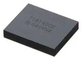
MYC0409-NA-D
DC/DC POL Converter, Adjustable, Charge Pump, 20 V to 60 V in, 5 V to 15V /6A out, LGA-52
⚠️ Reference pricing provided. In case of supply shortages, we will connect you with our trusted procurement partners to ensure your project's continuity.
- Manufacturer: MURATA POWER SOLUTIONS
- Product type: DC / DC Non Isolated Board Mount Converters - Adjustable Output
- Available until stocks are exhausted Alternative available
- MSL: -
- SVHC: No SVHC (07-Nov-2024)
- Depth: 11.5mm
- Width: 9.5mm
- Height: 2.1mm
- Topology: Charge Pump
- No. of Pins: 52Pins
- Product Range: UltraCP MYC Series
- No. of Outputs: 1 Output
- Output Current: 6A
- Output Power Max: -
- Input Voltage Max: 60V
- Input Voltage Min: 20V
- Output Current Max: 6A
- Output Voltage Max: 15V
- Output Voltage Min: 5V
- Switching Frequency: 270kHz
- Input Voltage DC Max: 60V
- Input Voltage DC Min: 20V
- DC / DC Converter Type: Charge Pump, Module
- DC / DC Converter IC Case: LGA
- Operating Temperature Max: 105°C
- Power Supply Applications: ITE & Industrial
- DC / DC Converter Output Type: Adjustable
| Delivery and price | |
|---|---|
| Units per pack | 10 |
| Price | 16.34 € |
| Current stock | 25+ |
| Lead time | 30 days |
Datasheet

Document Category: Advanced Datasheet / Subject to change

## **UltraCP™   MYC0409**

Ultra-thin High Efficiency 72W DCDC converter module

## **Product Description**

The **MYC0409** is an Ultra-thin High Efficiency integrated power solution which combines a 72W DC-DC converter with components. This total power solution can be used in a system without loop compensation and with just three external components in the minimum case.

This fully integrated module provides up to 96.5% efficiency despite small and thin 11.5mm x 9.5mm x 2.0mm LGA package. Murata’s easy-to-use module pinout design allows simple power layout and maximizing efficiency by minimize routing parasitic resistance.

## **Efficiency**

Ta=25degC.

This module is fixed divide-by-4 conversion ratio from input voltage to output voltage. Input voltage range of 20V to 60V supports 48V bus systems.

- Wide input voltage 20 to 60V (DIV4)

- Suitable for 48V bus systems

- Efficiency up to 96.5% Up to 95.0% Efficiency with 48VIN/6A

- Up to 6A

- Ultra-thin/small 11.5 x 9.5 x 2.0mm LGA package. (T=2.1mm MAX)

## **Features**

**Figure 1. Efficiency Plot**

## **Simplified Application**

- Open Drain Power-Good output

- Over-current and Over-temperature protection

- Compensation loop-less Charge Pump

- Synchronizes to an external clock

- Stackable up to 4 modules

## **Typical Applications**

- Data centers/servers

- Networking equipment

- Base stations

- Optical equipment

- Test equipment

- LED signage

**Figure 2. Simplified Circuit Diagram**

**http://www.murata.com/products/power**

Document Number: D90DH00151  /  Export Control Code: X0863 MYC0409   RevA01 (DEC-2021)       Page 1 of 31

Copyright ©2021 Murata Manufacturing Co., Ltd. All rights reserved. Specifications are subject to change without notice.

Document Category: Advanced Datasheet / Subject to change

## **UltraCP™   MYC0409**

Ultra-thin High Efficiency 72W DCDC converter module

## **Table of Contents**

**==> picture [234 x 399] intentionally omitted <==**

**----- Start of picture text -----**<br>
||||
|---|---|---|
|Product Description ....................................................... 1|
|Features .......................................................................... 1|
|Typical Applications ...................................................... 1|
|Efficiency ........................................................................ 1|
|Simplified Application .................................................... 1|
|Absolute Maximum Ratings|[(1)]|...................................... 3|
|Recommended Operating Conditions|[(1)]|...................... 3|
|Package Thermal Characteristics|[(1,2)]|........................... 3|
|Electrical Characteristics|[(1)]|........................................... 4|
|Electrical Characteristics Table|............................................... 4|
|Pin Configuration ........................................................... 6|
|Pin Description ............................................................... 6|
|Application Circuit ......................................................... 7|
|Typical Performance Characteristic ............................. 8|
|Efficiency .................................................................................... 8|
|Thermal Deratings (Reference Data) .......................... 10|
|Detailed Description ..................................................... 11|
|Startup – EN, VIN relationship. ................................................. 11|
|Enable (EN) .............................................................................. 12|
|Input Under-voltage Lockout (UVLO) ........................................ 12|
|Pre-charge Operation ............................................................... 12|
|Soft-Start Operation .................................................................. 12|
|PGOOD Operation ................................................................... 12|
|External/Internal Clock Modes and SYNCSEL Pin .................... 14|
|Protections|[(1)]|................................................................ 14|
|VIN Under-voltage and Thermal Shutdown Faults .................... 15|
|ILOAD Overcurrent Protection .................................................. 15|
|VOUT Under-voltage Protection ............................................... 15|
|Soft-start Timeout ..................................................................... 15|
|PGOOD Low Detection ............................................................. 16|
|Application Information ............................................... 16|

**----- End of picture text -----**<br>


Charge Pump architecture Basics ............................................. 16 **Application Performance ............................................. 18 Application Schematic ................................................. 18 Application Circuit Part List ........................................ 19 Application Board Example ......................................... 19 Component Selection ................................................... 20** Input Capacitor ......................................................................... 20 Output Capacitor ...................................................................... 20 Input Fuse ................................................................................ 20 **Parallel operation ......................................................... 20** Current and Thermal Balance ................................................... 20 Pin connections for parallel operation ....................................... 20 **Charge Pump architecture and important notice ...... 22** Hard Short Circuit Condition ..................................................... 22 Soft start and capacitors charge balancing ............................... 22 Reverse Direction Current Flow and Operation ......................... 23 **Packaging Information ................................................. 24** Moisture Sensitivity Level ......................................................... 24 Package Drawing ..................................................................... 24 Recommended board land pattern ............................................ 25 Top Marking Specification ......................................................... 26 **Tape and Reel Specification ........................................ 27 Order Codes .................................................................. 29 Notices ............................................................................. 30 CAUTION ................................................................... 30** Limitation of Applications ................................................................. 30 Note ................................................................................. 30 Preliminary Specification........................................................... 30 Sales contact ................................................................................ 30 **Disclaimers ....................................................................... 30** Patent Statement ........................................................................... 31 **Copyright and Trademark .................................................... 31**

**http://www.murata.com/products/power**

Document Number: D90DH00151  /  Export Control Code: X0863 MYC0409   RevA01 (DEC-2021)       Page 2 of 31

Copyright ©2021 Murata Manufacturing Co., Ltd. All rights reserved. Specifications are subject to change without notice.

## **Absolute Maximum Ratings[(1) ]**

|**PARAMETER**|**MIN**|**MAX**|**UNITS**|
|---|---|---|---|
|VIN|-0.3|61|V|
|EN|-0.3|VIN+0.3|V|
|SYNC, SYNCSEL, PGOOD|-0.3|5.5|V|
|VOUT|-0.3|VIN/4<br>+0.1|V|
|IOUT|0|8|A|
|StorageTemperature|-40|125|°C|
|Soldering / Reflow temperature|-|260|°C|
|ESD Tolerance,HBM(2)|1000|-|V|


_Notes:_

_(1) The application of any stress beyond those listed under “Absolute Maximum Ratings” may cause permanent damage to the device, and exposure at any of these ratings for extended periods may reduce the reliability of the device. The above “Absolute Maximum Ratings” are stress ratings only; the notation of these conditions does not imply functional operation of the device at these or any other conditions that fall outside of the range identified by the operational sections of this specification. (2) Human body model, per the JEDEC standard JS-001-2012._

## **Table 1. Absolute Maximum Ratings**

## **Recommended Operating Conditions[(1)]**

|**PARAMETER**|**MIN**|**MAX**|**UNITS**|
|---|---|---|---|
|VIN|20|60|V|
|Ambient Temperature|-40|105|°C|
|Junction Temperature(2)|-40|120|°C|
|Load Current|0|6|A|
|_Notes:_||||
|_(1) Device should not be operated outside the operating conditions. The reliability is tested at the maximum voltage of the recommended_||||
|_operating condition. Above of recommended operation may reduce reliability of the device._||||
|_(2) See the temperature derating curves in the thermal deratings. However, do not condensate._||||


## **Table 2. Recommended Operating Conditions**

## **Package Thermal Characteristics[(1,2) ]**

|**PARAMETER**|**TYP**|**UNITS**|
|---|---|---|
|Θjct<br>Junction-case-top at heat Junction|15.9|°C/W|
|Θjcb<br>Junction-case-bottomatheat Junction|4.7|°C/W|
|_Notes:_|||
|_(1) Package thermal characteristics and performance are measured and reported in a manner consistent with the JEDEC standards_|||
|_JESD51-8 and JESD51-12._|||
|_(2) Junction-to-Ambient Thermal Resistance (ƟJA) is a function not only of the IC, but it is also extremely sensitive to the environment_|||
|_which includes, but is not limited to, board thickness, planes, copper weight / routes, and air flow. Attention to the board layout is_|||
|_necessary to realize expected thermal performance_|||


**Table 3. Package Thermal Characteristics**

**http://www.murata.com/products/power** ~~ST~~ Copyright ©2021 Murata Manufacturing Co., Ltd. All rights reserved. Specifications are subject to change without notice.

Document Number: D90DH00151  /  Export Control Code: X0863 MYC0409   RevA01 (DEC-2021)       Page 3 of 31

## **Electrical Characteristics**[(1) ]

## **Electrical Characteristics Table**

## _VIN=48V, IOUT=6A, Ta = 25°C, unless otherwise noted_

|**PARAMETER**|**SYMBOL**|**CONDITIONS**|**MIN**|**TYP**|**MAX**|**UNITS**|
|---|---|---|---|---|---|---|
|**INPUT SUPPLY**|||||||
|VIN|VIN||20|48|60|V|
|VIN Start-upSlew rate(2)|VINSR||0.2|-|-|V/ms|
|VIN<br>Under<br>Voltage<br>Lockout<br>Threshold, VIN rising|VIUVLO|IOUT=0A|-|18.1|-|V|
|VIN<br>Under<br>Voltage<br>Lockout<br>Hysteresis|VIUVHYS|IOUT=0A|-|0.9|-|V|
|VIN Switchingsupplycurrent|IVINSW|VIN=48V,No Load|-|11|-|mA|
||||||||
|**ENABLE INPUT (EN PIN)**|||||||
|Enable Threshold High(2)|VTENH||1.5|-|-|V|
|Enable Threshold Low(2)|VTENL||-|-|0.6|V|
|Enable Input risingduration(2)|TREN|0V to VTENH|-|-|1|ms|
||||||||
|**POWER GOOD**|||||||
|PGOOD output pulldown low<br>level(2)||IPGOOD=20mA|-|-|0.25|V|
|PGOOD input high voltage(2)|PGINH||0.9|-|-|V|
|PGOOD input low voltage(2)|PGINL||-|-|0.7|V|
|PGOOD Hysteresis|PGHYS||-|0.4|-|V|
|PGOOD VOUT Threshold|PGVOTH|VOUT Rising, No Fault|-|0.95*<br>VIN/4|-|V|
|PGOOD<br>Released<br>VOUT<br>threshold|PGVOR|VOUT Falling after PGOOD=H|-|0.8*<br>VIN/4|-|V|
||||||||
|**I/O INPUT(SYNCSEL PIN)**|||||||
|Threshold High(2)|VTIOH||1.1|-|-|V|
|Threshold Low(2)|VTIOL||-|-|0.4|V|
||||||||
|**OUTPUT**|||||||
|EfficiencyPeak||IOUT=2.4A|-|96.5|-|%|
|EfficiencyFull Load||IOUT=6A|-|95.0|-|%|
|SwitchingFrequency|FSW||-|270|-|kHz|
|Soft Start Input Current Limit|IVINSS||-|134|-|mA|
|Soft Start timeout duration|TSSTO||-|100|-|msec|
|Output Current(Continuous)|IOUT Cont|Inside recommended OP range|-|-|6|A|
|VOUT Voltage|VOUT|VIN=48V, Full load condition, DC|-|95.5%*<br>VIN/4|-|V|
|Total external<br>Output capacitance(2)|COUT||44|-|400|uF|
|Total external<br>Output capacitance<br>with Parallel operation(2)|COUTP|n=Parallel devices numbers|44*n|-|400|uF|
||||||||
|**PROTECTION**|||||||
|Thermal Shutdown Threshold(2)|TSD|Temperature rising|125|150|-|°C|
|Thermal Shutdown Hysteresis|TSDHYS||-|16|-|°C|
|Over Current Protection|IOCP||-|10|-|A|
||||||||
|**ENVIRONMETAL**|||||||
|Moisture SensitivityLevel|MSL|||3|||
|_Notes:_|||||||


**http://www.murata.com/products/power** ~~ST~~

Document Number: D90DH00151  /  Export Control Code: X0863 MYC0409   RevA01 (DEC-2021)       Page 4 of 31

Copyright ©2021 Murata Manufacturing Co., Ltd. All rights reserved. Specifications are subject to change without notice.

## **Electrical Characteristics Table**

## _VIN=48V, IOUT=6A, Ta = 25°C, unless otherwise noted_

## **PARAMETER SYMBOL CONDITIONS MIN TYP MAX UNITS**

_(1) Min/Max specifications are 100% production tested at TA=25 °C, unless otherwise noted. Limits over the operating range are guaranteed by design._

_(2) Guaranteed by Design_

## **Table 4. Electric Characterisics Table**

**http://www.murata.com/products/power** ~~ST~~ Copyright ©2021 Murata Manufacturing Co., Ltd. All rights reserved. Specifications are subject to change without notice.

Document Number: D90DH00151  /  Export Control Code: X0863 MYC0409   RevA01 (DEC-2021)       Page 5 of 31

## **Pin Configuration**

|G1<br>VIN<br>G2<br>DNC<br>G3<br>EN<br>PI LILI|G1<br>VIN<br>G2<br>DNC<br>G3<br>EN<br>PI LILI|G1<br>VIN<br>G2<br>DNC<br>G3<br>EN<br>PI LILI|G4<br>DNC<br> LI|G4<br>DNC<br> LI|G5<br>GND<br>G6<br>GND<br>G7<br>GND<br> WI|G8<br>GND|
|---|---|---|---|---|---|---|
||F1<br>VIN<br>F2<br>DNC<br>EJ Ld||||F5<br>GND<br>F6<br>GND<br>F7<br>GND<br>F8<br>GND<br>PILILI<br>Ld||
||E1<br>VIN<br>E2<br>DNC<br>E3<br>GND<br>PJ LILI||E4<br>GND<br> LI||E5<br>GND<br>E6<br>GND<br>E7<br>GND<br>E8<br>GND<br> WILL||
||D1<br>DNC<br>D2<br>GND<br>D3<br>GND<br>PJLILI||D4<br>GND<br> LI||D5<br>GND<br>D6<br>GND<br>D7<br>GND<br>td|D8<br>VOUT|
||C1<br>GND<br>C2<br>GND<br>C3<br>GND<br>PF LIU||C4<br>GND<br> LJUtd||C5<br>GND<br>C6<br>GND<br>C7<br>GND<br>C8<br>VOUT<br>Utd||
||B1<br>GND<br>B2<br>GND<br>ae||||B5<br>GND<br>B6<br>GND<br>B7<br>GND<br>B8<br>VOUT<br>PILILI<br>Ld||
|A1<br>GND<br>A2<br>DNC<br>A3<br>GND<br>PJLILI|||A4<br>PGOOD<br>LU||A5<br>SYNC<br>A6<br>SYNC<br>SEL<br>A7<br>GND<br>Lt|A8<br>VOUT|


**Figure 3. Module Terminals (Top view)**

## **Pin Description**

|**PIN No.**<br>**Name**<br>**Description**|**PIN No.**<br>**Name**<br>**Description**|**PIN No.**<br>**Name**<br>**Description**|
|---|---|---|
|A1, A3, A7, B1, B2, B5-B7, C1-C7,<br>D2-D7, E3-E8, F5-F8, G5-G8<br>GND<br>Ground for power and thermal.<br>Please connect ground plane in low impedance.|||
|E1, F1, G1<br>VIN<br>Power input terminal|||
|A8, B8, C8, D8<br>VOUT<br>Power output terminal|||
|G3<br>EN<br>Part Enable terminal. Do not leave this terminal open.<br>HIGH=ON / LOW=OFF|||
|A5<br>SYNC<br>CLOCK IN / OUT terminal. Direction is configurable by SYNCSEL terminal<br>potential.|||
|A6<br>SYNCSEL<br>SYNC terminal control.<br>LOW=CLKOUT, HI-Z=CLKIN.|||
|A4<br>PGOOD<br>Power GOOD terminal. Connect 10KOhms resistor from PGOOD to an<br>external bus voltage between 3.3V and 5.5V. When left open, PGOOD pulls<br>up to the internal VDD voltage of 1.2V.|||
|A2, D1, E2, F2, G2, G4|DNC|Do not connect pins electrically. Those pins must connect to the board with<br>solder but must be left floating electrically each other.|


**Table 5. Pin Description**

**http://www.murata.com/products/power**

Document Number: D90DH00151  /  Export Control Code: X0863 MYC0409   RevA01 (DEC-2021)       Page 6 of 31

Copyright ©2021 Murata Manufacturing Co., Ltd. All rights reserved. Specifications are subject to change without notice.

## **Application Circuit**

**Figure 5. Application Circuit**

**http://www.murata.com/products/power** Copyright ©2021 Murata Manufacturing Co., Ltd. All rights reserved. Specifications are subject to change without notice.

Document Number: D90DH00151  /  Export Control Code: X0863 MYC0409   RevA01 (DEC-2021)       Page 7 of 31

## **Typical Performance Characteristic**

In this document, all characteristics are measured with application board which is shown in Fig.25. The board is under Ta=25degC with no airflow unless otherwise noted.

## **Efficiency**

**Figure 6. Efficiency (Linear, Log scale)**

Startup waveform with VIN=48V, No load, Ta=25degC. Tek Run Sample Degs

**Figure 7. Start-up Waveform**

Shutdown waveform with VIN=48V, IOUT=6A, Ta=25degC. Tek Preview Sample Degs aSAe 20ST

**Figure 8. Shutdown Waveform**

Document Number: D90DH00151  /  Export Control Code: X0863 MYC0409   RevA01 (DEC-2021)       Page 8 of 31

**http://www.murata.com/products/power** Copyright ©2021 Murata Manufacturing Co., Ltd. All rights reserved. Specifications are subject to change without notice.

VOUT ripple waveform with VIN=48V, IOUT=6A, Ta=25degC.

**Figure 9. VOUT ripple Waveform**

Load transient response waveform with VIN=48V, IOUT=0A to 6A, Ta=25degC. Tek Stopped _ 14 Acs - 18 Ape 21.14:00:11

**Figure 10. Load transient response Waveform (0A to 6A)**

Load transient response waveform with VIN=48V, IOUT=6A to 0A, Ta=25degC. Tek Stopped BRAgs —_ __1S Ape 21 14:00:41

**Figure 11. Load transient response Waveform (6A to 0A)**

**http://www.murata.com/products/power** Copyright ©2021 Murata Manufacturing Co., Ltd. All rights reserved. Specifications are subject to change without notice.

Document Number: D90DH00151  /  Export Control Code: X0863 MYC0409   RevA01 (DEC-2021)       Page 9 of 31

## **Thermal Deratings (Reference Data)**

Thermal Deratings with VIN=48V (Reference Data)

**Figure 12. Thermal Deratings (VIN=48V)**

Thermal Deratings with VIN=54V (Reference Data)

**Figure 13. Thermal Deratings (VIN=54V)**

Thermal deratings are evaluated in following condition. `・` The product is mounted on 114.5 x 101.5 x 1.6mm (Layer1, 4: 2oz Layer2, 3: 1oz copper) FR-4 board. Surface temperature of the product: 116°C max.

**http://www.murata.com/products/power** Copyright ©2021 Murata Manufacturing Co., Ltd. All rights reserved. Specifications are subject to change without notice.

Document Number: D90DH00151  /  Export Control Code: X0863 MYC0409   RevA01 (DEC-2021)       Page 10 of 31

## **Detailed Description**

The MYC0409 is a divide-by-4, two-phase charge pump-based DC-DC converter, so any change in input voltage will be reflected at the output.

The MYC0409 can be powered from input voltage ranges from 20V to 60V. The output voltage range supported is 5V to 15V with load currents of 6A

The SYNCSEL pin can be tied to ground or by left floating, if tied to ground then the device will use an internal clock and this clock signal will appear at the SYNC pin. If left floating, then the SYNC pin will act as an input. Please refer to Table 7 for details. The pin configurations are sampled when the MYC0409 starts up and before the charge pump stage is enabled. The configuration pins are not designed to be driven dynamically, so they should be in a fixed state at power up.

## **Startup – EN, VIN relationship.**

The MYC0409 has an enable input pin, EN, which is designed to be compatible with typical low-voltage digital I/O levels so that it can be easily driven by an external controller. EN can also be connected to the VIN pin. If external power sequencing or control is not required, EN should be tied to VIN and not left open.

If the EN pin is held low until VIN has reached its nominal voltage, the MYC0409 follows the initialization sequence shown in Figure 14.

**Figure 14. Initialization Sequence**

**http://www.murata.com/products/power**

Document Number: D90DH00151  /  Export Control Code: X0863 MYC0409   RevA01 (DEC-2021)       Page 11 of 31

Copyright ©2021 Murata Manufacturing Co., Ltd. All rights reserved. Specifications are subject to change without notice.

## **Enable (EN)**

The MYC0409 is enabled by an active-high EN input pin when a voltage greater than 1.5V is applied. The MYC0409 is disabled when the voltage at the EN pin falls below 0.6V. The EN pin can be shorted to the VIN pin to automatically enable the part with a minimal number of external components and PCB routing. When multiple MYC0409s are used in parallel, all their EN pins must be connected to a single enable signal. Scope plots showing the enable and disable behavior are shown in Figure 7 and Figure 8.

## **Input Under-voltage Lockout (UVLO)**

The MYC0409 provides continuous monitoring of the VIN input using a fixed under-voltage lockout threshold. The MYC0409 is enabled when the VIN voltage rises above 18.1V typical. When the VIN voltage falls below the fixed under-voltage lockout threshold plus additional 0.9V hysteresis, charge pump switching is disabled.

## **Pre-charge Operation**

Before enabling the soft start switching sequence, the MYC0409 pre-charges the internal flying capacitors to a balanced state based upon the divider ratio. This is done so that when the soft-start phase commences, the voltage across the capacitors is at their nominal voltage and known state. Note that the adaptive pre-charge system takes pre-charging time depending on the external voltages present on the circuit.

## **Soft-Start Operation**

After the pre-charge phase is completed, the device enters soft-start mode and charges the output capacitor at 134 mA typical value input current. It exits the state when the VOUT voltage has reached within 5% of the target voltage, which is VIN divided by 4. The PGOOD pin can go high at the same time. Figure 7 shows a typical powerup sequence.

As the device goes through a soft-start sequence, full load currents should not be applied to the device until the PGOOD pin is high. If a full load is connected before this, the device will not start up. If the output current is loaded, VOUT may not reach the target during the soft-start phase. As a result, the system detects soft-start timeout, latches off the device and then requires the EN pin to be toggled to restart. The soft-start timeout is 100 msec typical value. A similar situation can also happen if the charge pump has too much COUT capacitance.

## **PGOOD Operation**

The power good pin is a bi-directional open drain pin. When the output voltage is above 95% of VIN /4, the PGOOD pull-down FET is turned off to allow the external pull-up resistor to pull up the node. The PGOOD pin must be pulled up externally. If another device or digital I/O is also pulling down on this pin, the MYC0409 remains in soft-start mode, and high-power mode is not enabled. When MYC0409 allows PGOOD to be pulled high, the charge pump is ready to support the full load current.

When multiple MYC0409s are used in parallel, all their PGOOD pins must be connected. In this case, all MYC0409s must complete soft-start before PGOOD is asserted and full power operation is allowed. In the event of a fault at one or more parallel MYC0409s, the PGOOD pin will be pulled low by the faulted MYC0409s.

Note that the PGOOD pin of a disabled device will NOT be pulled low if the device is not enabled. In effect, if EN=0, the PGOOD pin should be ignored. Table 6 shows the PGOOD pin table and Figure15 shows PGOOD Sequence Diagram. VOUT pre-biased condition would enable PGOOD function to pull low if the part enabled.

Figure16 shows an example of PGOOD Application Circuit. If there is not 3.3V-5V rail, PGOOD can be pulled up by divided VOUT. Using 100kohm and 47kohm with 1% tolerance to the VOUT dividing resistors can support wide VIN range. Note that PGOOD voltage varies with VOUT voltage with this case.

**http://www.murata.com/products/power** ~~ST~~ Copyright ©2021 Murata Manufacturing Co., Ltd. All rights reserved. Specifications are subject to change without notice.

Document Number: D90DH00151  /  Export Control Code: X0863 MYC0409   RevA01 (DEC-2021)       Page 12 of 31

|**VIN**<br>**EN**|**STATE**|**PGOOD**|
|---|---|---|
|VIN≦ UVLO<br>X|X|X**(1)**|
|VIN>UVLO<br>LOW|Shut-down|HIGH**(2)(3)(4)**|
|VIN>UVLO<br>HIGH|After Start-upand Normal(fault free)operation|HIGH**(5)**|
||Others|LOW|
|_Notes:_|||
|_(1) If VIN_≦_UVLO, the PGOOD should be ignored._|||
|_(2) It is pulled HIGH when the module is in stopped state shut-down._|||
|_(3) EN signal changes from HIGH to LOW (Shut down period), it indicates Low for 60ms(Typical). After that, the PGOOD is pulled HIGH._|||
|_(4) In the case of PGOOD is pulled up by divided VOUT, it indicates Low._|||
|_(5) It indicates LOW during soft-start operation._|||


**Table 6. PGOOD Pin Table**

**Figure 15. PGOOD Sequence Diagram**

**Figure 16. PGOOD Application Circuit**

**http://www.murata.com/products/power**

Document Number: D90DH00151  /  Export Control Code: X0863 MYC0409   RevA01 (DEC-2021)       Page 13 of 31

Copyright ©2021 Murata Manufacturing Co., Ltd. All rights reserved. Specifications are subject to change without notice.

## **External/Internal Clock Modes and SYNCSEL Pin**

In most applications, the MYC0409 operates using an internal oscillator. Table 7 shows the SYNC pin table.

|**DETECTOR**<br>**SYNC**<br>**EFFECT OF FAULT**|**DETECTOR**<br>**SYNC**<br>**EFFECT OF FAULT**|**DETECTOR**<br>**SYNC**<br>**EFFECT OF FAULT**|
|---|---|---|
|GND<br>Output<br>Internalclock is sent to the SYNC pinas anoutput.|||
|OPEN<br>(HI-Z)|Input|An external clock can be applied to the sync input.<br>If no clock in, internal clock is used.|


## **Table 7. SYNC Pin Table**

The charge pump is operated at half frequency of the SYNC pin input/output clock. Because MYC0409 internal components are optimized for efficiency with the internal oscillator frequency, injecting an external clock is not recommended for single-unit applications. If configured to use an external clock (SYNCSEL=open circuit), and the external clock stops or is not present for some reason, an internal watchdog detects the missing clock and causes MYC0409 to swap back to use of the internal clock source. When the expected external clock source resumes, the MYC0409 reverts to using the external clock.

When the SYNCSEL pin is tied to GND, the internal clock is present on the SYNC pin.

For parallel operation, SYNCSEL pin on one of the paralleled modules should be GND to provide the clock for the others, the other paralleled modules should be left floating to receive the shared clock to get all synced up.

## **Protections[(1)]**

MYC0409 is a high power device. To protect both the system, and the internal circuitry of MYC0409, there are multiple fault detection circuits built in. Table 8 shows a summary of the various protection modes.

|**DETECTOR**<br>**LATCHED OFF OR**<br>**AUTOMATIC RETRY**<br>**RESPONSE**<br>**TIME**<br>**EFFECT OF FAULT**|**DETECTOR**<br>**LATCHED OFF OR**<br>**AUTOMATIC RETRY**<br>**RESPONSE**<br>**TIME**<br>**EFFECT OF FAULT**|**DETECTOR**<br>**LATCHED OFF OR**<br>**AUTOMATIC RETRY**<br>**RESPONSE**<br>**TIME**<br>**EFFECT OF FAULT**|**DETECTOR**<br>**LATCHED OFF OR**<br>**AUTOMATIC RETRY**<br>**RESPONSE**<br>**TIME**<br>**EFFECT OF FAULT**|
|---|---|---|---|
|Over<br>temperature<br>Automatic retry<br>µs<br>PGOOD goes low and the power stage switches off until the<br>temperature reduces under the hysteresis threshold. At this point, the<br>device automatically restarts. The device needs to restart into no load<br>to automatically restart.||||
|VIN<br>under<br>voltage<br>Automatic retry<br>µs<br>PGOOD goes low and the charge pump is disabled until VIN returns<br>above the UVLO threshold and enabled. The device needs to restart<br>into no load to automatically restart.||||
|ILOAD<br>over<br>current<br>Automatic retry<br>µs<br>If the load current exceeds the over-current limit, PGOOD goes low<br>and the charge pump is disabled for a certain period to cool down. If<br>the device is still over current after the cooldown period, after the<br>cooldown period it automatically restarts.||||
|ILOAD<br>short<br>circuit<br>Latched off<br>us<br>If the load current exceedsthe short-current limit, the device is<br>immediately latched off and shuts down. EN must be toggled to<br>restart the device.||||
|Soft-start<br>timeout<br>Latched off<br>µs<br>If VOUT does not reach the target voltage of VIN divided by 4 within<br>the soft start timeout period, the device shuts down and EN must be<br>toggled to restart it.||||
|PGOOD<br>held<br>low<br>Automatic retry<br>µs<br>If the charge pump is operating at full power and if PGOOD is<br>pulled down externally, the device enters soft-start mode. If the<br>PGOOD pin is held low for less than the soft-start period, the<br>charge pump returns to full power operation. If the PGOOD pin is<br>held low for longer than the soft-start duration, the charge pump<br>completes a soft-start cycle before returning to normal operation<br>and shouldnot beloaded during this period.||||
|VOUT<br>under-<br>voltage|Automatic retry|µs|If the output of the device is under the VOUT threshold, the<br>PGOOD pin is pulled low. The device will switch off and enter a<br>cooldown period. After the cool down period the charge pump will<br>restart into soft start mode.|


**Table 8. Protections**

_Note: (1) Protections are designed to prevent any damages or issues on the module as a best effort service. This will not guarantee safety or no damages in your system. Murata highly recommends having the primary protection like adding Fuse and regarding those protections as supportive functions in your systems._

**http://www.murata.com/products/power** ~~ST~~ Copyright ©2021 Murata Manufacturing Co., Ltd. All rights reserved. Specifications are subject to change without notice.

Document Number: D90DH00151  /  Export Control Code: X0863 MYC0409   RevA01 (DEC-2021)       Page 14 of 31

## **VIN Under-voltage and Thermal Shutdown Faults**

The VIN under-voltage and thermal shutdown faults are grouped together purely because the effect they have on the charge pump is similar. If either of these faults is present when the charge pump is first enabled, the charge pump cannot start up.

The charge pump holds in this state until both faults are clear, regardless of how long this takes.

VIN under-voltage and thermal shutdown faults are considered “persistent” as they will hold the charge pump disabled until the fault clears.

In the case of VIN under-voltage, it is unlikely that the charge pump will be able to support the full load current when VIN (and therefore VOUT too) is too low. Because it is not desirable for MYC0409 or for the load to operate in this condition, the charge pump will hold off waiting for VIN to improve/recover.

An over-temperature fault is likely to occur only when MYC0409 is dissipating too much internal power, which normally results from some other fault condition such an overload condition. In the event of over-temperature, MYC0409 may start to drift out of guaranteed performance specifications, which would be undesirable for the system. To recover from over-temperature, the power dissipation in MYC0409 must be reduced to reduce the internal temperature.

When VIN under-voltage or an over-temperature fault are detected during normal operation, MYC0409 enters a controlled shutdown sequence with an unlimited cooldown period. When the faults clear, the MYC0409 enters a soft-start sequence.

## **ILOAD Overcurrent Protection**

Over-current protection operates by sensing the current being drawn from VIN. The over-current protection trips when MYC0409 is operated outside the recommended operating conditions. Typically, the device trips when the output current exceeds 10A Typical. The over-current protection has two separate protection methods.

- If the current exceeds the over current protection threshold of 10A Typical, then when triggered the device will enter a cooldown period and after this automatically restart. During this time the PGOOD pin is pulled low.

- If the current exceeds 15A Typical, the device immediately shuts down and latches off. During this time, the PGOOD pin is pulled low. To restart the device, the EN pin must be toggled.

MYC0409 reacts to over-current faults by entering a controlled shutdown sequence. The device is then latched off until EN is toggled. After enable is toggled and the pre-charge is complete, MYC0409 enters a normal soft-start sequence and attempts to restart. Note that some persistent fault conditions may prevent the charge pump from restarting successfully, for example, in the event of a hard fault to GND at VOUT.

## **VOUT Under-voltage Protection**

The VOUT under-voltage fault detector measures value at VOUT with the expected value derived from VIN/4. The VOUT under-voltage fault is designed to be slow and represents an averaged value. The VOUT under-voltage flag trips when VOUT goes below 80% of the target (VUVP).

The VOUT under-voltage detector trips when VOUT goes below 80% of the target voltage. It is important that external components are chosen so that the expected transient loads do not trip the VUVP threshold. In effect, the application should ensure that the load dependency causes a less than 20% deviation from the nominal VOUT.

## **Soft-start Timeout**

When MYC0409 first tries to supply power to the load, it uses a soft-start circuit so that the power level is limited. Using a soft start has no significant side effects if the start-up is “normal”.

If MYC0409 starts up into a fault, the soft-start helps manage the power being supplied to the fault as well as limiting the power dissipation in MYC0409. In normal, fault-free operation, the soft-start timeout should be invisible if the soft-start current is able to ramp VOUT to the target voltage inside 100 ms. In the event of a fault, the softstart timeout occurs when VOUT does not ramp to the target voltage in the expected time. In this case, the softstart timeout causes power to the load to be stopped and MYC0409 to enter a controlled shutdown sequence. The device then latches off, and EN must be toggled to restart it.

**http://www.murata.com/products/power** ~~ST~~ Copyright ©2021 Murata Manufacturing Co., Ltd. All rights reserved. Specifications are subject to change without notice.

Document Number: D90DH00151  /  Export Control Code: X0863 MYC0409   RevA01 (DEC-2021)       Page 15 of 31

## **PGOOD Low Detection**

In a stand-alone MYC0409 implementation, the PGOOD signal will likely have only one driver. When MYC0409 is ready for full power, PGOOD goes high and stays high for as long as the single MYC0409 remains enabled and fault-free.

In parallel operation, the PGOOD signal must be connected in a wired OR configuration with the other devices. When all devices are ready for full power, the PGOOD signal goes high. In the event of a fault, the PGOOD signal is pulled low and switches off all the parallel devices. EN must then be toggled to restart the devices.

## **Application Information**

Charge Pump based DCDC converter is the high efficiency bus converter which doesn’t have the regulation capability. Because of its architecture, there are some differences from conventional inductive buck converters. And some of the behaviors may cause critical issues if you use inappropriate way although it is as same way as the conventional buck converters.

## **Charge Pump architecture Basics**

Charge Pump is capacitive voltage converter which is configured by plural of switches and capacitors like shown in Figure17. The drawing shows divide by four configuration.

**Figure 17. Divide by Four Charge Pump Configuration**

Charge pump usually has two main switch states. Our UltraCP[TM] series also have the two main switch states shown in Figure18-A and Figure18-B.

**Figure 18-A. Divide by Four Charge Pump Phase One Configuration**

**http://www.murata.com/products/power**

Document Number: D90DH00151  /  Export Control Code: X0863 MYC0409   RevA01 (DEC-2021)       Page 16 of 31

Copyright ©2021 Murata Manufacturing Co., Ltd. All rights reserved. Specifications are subject to change without notice.

**Figure 18-B. Divide by Four Charge Pump Phase Two Configuration**

During phase one, flying capacitor of C1 will be connected between VIN and VOUT. And the C2 and C3 will be connected between VOUT and GND. In phase two, C1 and C2 will be connected between VOUT and GND. And the C3 will be connected between VOUT and GND. Fig.18 shows these two states of capacitor connection and charged voltage relationship. Once the charge pump finishing soft-start, each capacitor will have VIN/4, VIN*2/4 and VIN*3/4 voltage. This voltage will be maintained to keep switching between the phase one and the phase two. To improve the charge pump efficiency, increase the flying capacitor capacitance works well. Also, minimize switch resistance and parasitic resistance works, too. Our UltraCP[TM] series has optimized CFLY, power switch resistance and routing parasitic. Therefore, users wouldn’t need to care about such a detail.

**Figure 19. Divide by Four Charge Pump Capacitor Connection**

MYC0409 is based around a high efficiency, charge pump based DC-DC converter with an unregulated output voltage. Because of the architecture, there are some important characteristics which are different from conventional inductive buck converters. To avoid damage to the system, or the device, it is important to understand some of the key architecture differences compared to conventional buck converters. For the details, please refer the section of Charge Pump architecture and important notice.

**http://www.murata.com/products/power** Copyright ©2021 Murata Manufacturing Co., Ltd. All rights reserved. Specifications are subject to change without notice.

Document Number: D90DH00151  /  Export Control Code: X0863 MYC0409   RevA01 (DEC-2021)       Page 17 of 31

## **Application Performance**

Typical performance with the application board of Fig. 25 are shown in Fig. 20 to Fig. 23. Ta=25degC

**==> picture [367 x 185] intentionally omitted <==**

**----- Start of picture text -----**<br>
Figure 20. Efficiency Figure 21. Power Dissipation<br>0.0<br>dd = =<br>LT -3.0<br>aor= 4,<br>—,<br>E 60 vin=24V<br>= 70 || [—Vvin=36v]<br>—Vin=24V_ —Vin=36V >So .i —Vin=48V—_<br>—Vin=48V ———Vin=54V 9.9 || [——Vin=54V]<br>1 > 3 4 5 6 -10.0 0 1 2 3 4<br>lout [A] lout [A]<br>Figure 22. VOUT Voltage Figure 23. VOUT Voltage Drop Ratio<br>**----- End of picture text -----**<br>


## **Application Schematic**

An example of MYC0409 standalone schematic is shown in Fig.24. Please refer recommended circuit part list shown in Table 9.

**Figure 24. Application Schematic**

**http://www.murata.com/products/power** Copyright ©2021 Murata Manufacturing Co., Ltd. All rights reserved. Specifications are subject to change without notice.

Document Number: D90DH00151  /  Export Control Code: X0863 MYC0409   RevA01 (DEC-2021)       Page 18 of 31

## **Application Circuit Part List**

Example of the standard components are shown in Table 9. Components must be chosen referring the system requirement like Voltage, Temperature, etc.

|**REFERENCE**<br>**VALUE**<br>**DESCRIPTION**<br>**PART NUMBER**|**REFERENCE**<br>**VALUE**<br>**DESCRIPTION**<br>**PART NUMBER**|**REFERENCE**<br>**VALUE**<br>**DESCRIPTION**<br>**PART NUMBER**|**REFERENCE**<br>**VALUE**<br>**DESCRIPTION**<br>**PART NUMBER**|
|---|---|---|---|
|CIN1<br>100uF<br>Electrolysis Capacitor (Optional)(1)<br>-||||
|CIN2<br>4.7uF<br>Input Capacitor<br>Ceramic capacitor, 4.7µF, 100V,+/-10%, X7S<br>GRM31CC72A475KE11 (Murata)||||
|COUT<br>22uF x 2pcs<br>Output Capacitor<br>Ceramic capacitor, 22µF, 25V,+/-20%, X7S<br>GRM31CC71E226ME15 (Murata)||||
|RPG|10kohm|Pull up resistor for Power Good Indication<br>Chip resistor, 1/10W, 5%|RK73B1ETTP103J (KOA)|


**Table 9. Application Circuit Part List**

(1) If there is a non-negligible parasitic impedance between the power supply and the converter, such as during evaluation, the optional input capacitor "CIN1" may be required to reduce the impedance. The recommended optional capacitor is an example. Please consider the optimum value for the case. This capacitor is usually an aluminum electrolytic type. It isn't necessary to place the capacitor near the input terminal of the converter.

## **Application Board Example**

All reference data on this datasheet are taken with this board.

**Figure 25. Application board example**

~~————_~~ **http://www.murata.com/products/power** Copyright ©2021 Murata Manufacturing Co., Ltd. All rights reserved. Specifications are subject to change without notice.

Document Number: D90DH00151  /  Export Control Code: X0863 MYC0409   RevA01 (DEC-2021)       Page 19 of 31

## **Component Selection**

## **Input Capacitor**

The input capacitor is connected between VIN and GND. It is used to reduce the ripple on VIN. The input capacitor should be placed as close to the module as possible to reduce any parasitic inductance effects. The voltage rating of the capacitor needs to be as high as the absolute maximum voltage rating for the system and the effect of the capacitor voltage coefficient should be considered to determine the effective capacitance value at the applied VIN. Since the charge pump isn’t a regulator, ripple voltage on VIN will affect the output voltage.

## **Output Capacitor**

The output capacitor is used to reduce the ripple applied to the load at VOUT. The higher the capacitor value, the lower the ripple at VOUT. Increasing the output capacitor value will increase the soft start duration and might push the module to time out during soft start. Please take account into this to consider additional COUT value of your system. Following system’s input capacitance would be the COUT of MYC0409.

## **Input Fuse**

Certain applications and/or safety agencies may require fuses at the inputs of power conversion components. Fuses should also be used when there is the possibility of sustained input voltage reversal which is not currentlimited. For greatest safety, we recommend a fast blow fuse installed in the ungrounded input supply line. The installer must observe all relevant safety standards and regulations.

For safety agency approvals, install the converter in compliance with the end-user safety standard.

## **Parallel operation**

MYC0409 can be run in parallel in a multi-device configuration to increase output power as shown in figure 26. In parallel operation mode care and attention must be paid to some important things.

## **Current and Thermal Balance**

As with standard inductive DC-DC converters, a paralleled charge pump also must be taken care of the current/thermal balance. The MYC0409 provides divided voltage of the input voltage to its output. The output voltage relates the input voltage and the output voltage isn’t regulated. Therefore, the charge pump provides natural droop based on the equivalent output resistance (ROUT).

When the load applied to the paralleled charge pump modules, each output voltage of the modules starts to droop. The voltage drop from the ideal output voltage (VIN/DIV) is decided by (ROUT + parasitic resistance)*ILOAD. And the load current of each module is decided by the relationship of the (ROUT + parasitic resistance). For the charge pumps to load-share effectively attention should be paid to the layout to reduce the parasitic resistance of the output power tracks.

The MYC0409 is capable of up to 6A or 90W unless limited by other factors. Therefore, when in parallel operation imbalance in the load sharing caused by parasitic impedances can result in one module current limiting before another. This effect can restrict the total amount of power available to the system.

The power loss generated by the module results in heat rise in the module to maintain load sharing the modules should share the same thermal structure.

## **Pin connections for parallel operation**

Pin connection limitation is slightly different from the single module operation. Please follow below instruction and refer the Figure 26.

PGOOD output’s must be pulled up together and combined in a wire OR configuration. The load following the charge pump should not be switched on until all PGOOD are high and the load should immediately be switched off if any of the PGOOD outputs switch low after start up.

The SYNCSEL pin on one of the paralleled modules should be GND to provide the clock for the others, the other paralleled modules should be left floating to receive the shared clock to get all synced up.

**http://www.murata.com/products/power** ~~ST~~ Copyright ©2021 Murata Manufacturing Co., Ltd. All rights reserved. Specifications are subject to change without notice.

Document Number: D90DH00151  /  Export Control Code: X0863 MYC0409   RevA01 (DEC-2021)       Page 20 of 31

**Figure 26. Multi-module Application Circuit**

**http://www.murata.com/products/power** Copyright ©2021 Murata Manufacturing Co., Ltd. All rights reserved. Specifications are subject to change without notice.

Document Number: D90DH00151  /  Export Control Code: X0863 MYC0409   RevA01 (DEC-2021)       Page 21 of 31

## **Charge Pump architecture and important notice**

MYC0409 uses multiple, low impedance, switches to take advantage of the higher energy density available in capacitors (compared to inductors) to transfer power. The keys to optimizing charge pump efficiency include (i) reducing charge redistribution losses and (ii) minimizing thermal losses. MYC0409 reduce the charge redistribution loss with patented ‘almost loss-less’ architectures. The thermal losses are minimized by using lower voltage rated (internal) power FETs which take advantage of the reduced voltage as the input supply gets divided.

These two key features make MYC0409 very efficient. In exchange for the high efficiency, some of the differences to conventional buck converters need to be recognized to avoid permanent damage to the device.

Figure 27(A) shows an inductive regulator called a buck converter. There is an inductor between switching node to VOUT, so it would be prevented transient change of current when a hard short happened.

For Figure 27(B), it would be high di/dt condition with a hard short because MYC0409 does not have a large inductor but has low impedance of power FETs. In general, inductance would be reduced the current slope of inductor and impedance power FETs would be reduced peak current. Therefore, “Hard Short Circuit Condition” is written as bellow.

**(A) Inductive Regulator (B) Charge Pump Regulator**

**Figure 27. Inductive regulator and Charge pump**

## **Hard Short Circuit Condition**

MYC0409 is a capacitive DC-DC converter and has low inductance at the output to optimize efficiency. As a result of the low output inductance, a hard short at this product output can result in a di/dt condition which can be much higher than a conventional, inductive, buck converter would allow.

MYC0409 has a built-in output current protection. However, hard output short circuits with very low impedance may cause permanent damage to the device and should be avoided. If such faults needed to be considered, it may be necessary to add primary protection (external to the device) to ensure adequate protection of the device and the condition might be vary over the environment and use cases.

## **Soft start and capacitors charge balancing**

The charge pump is an open-loop capacitive DC-DC converter. The output voltage is generated using “flying” capacitors (“CFLY") which move charge from one voltage level to another. The voltage across the flying capacitors in normal operation will be limited to VOUT. The voltage balancing between, and across, the flying capacitors is important to maintain stability. Murata’s charge pump has several internal states which specifically enhance stability including “pre-charge” and “soft-start”. During pre-charge, each of the CFLY capacitors are charged to the appropriate DC voltage bias level (depending on VOUT) to ensure a balanced state at start-up. During soft-start, the charge pump starts switching with a controlled current (134mA typ. input current) to ramp VOUT to the target voltage (depending on VIN). The controlled start-up avoids in-rush current and EMI issues during turn on and ensures VOUT reaches VIN/4*95% before full power operation is enabled. As a further safety measure the softstart time is also monitored to ensure the system does not contain any unexpected leakage paths (like VOUT or CFLY shorts). As a result of the limited soft-start current, the system will not support starting up into a full power load. The PGOOD pin will indicate the system is ready for full load (when soft-start has finished, and VOUT has reached at least 95% of the nominal target voltage). The soft-start timeout protection also means that the maximum output capacitance should be limited for reliable startup. Increasing COUT beyond the recommended level may mean that the charge pump fails to start-up.

Document Number: D90DH00151  /  Export Control Code: X0863 MYC0409   RevA01 (DEC-2021)       Page 22 of 31

~~ee~~ **http://www.murata.com/products/power**

**http://www.murata.com/products/power** Copyright ©2021 Murata Manufacturing Co., Ltd. All rights reserved. Specifications are subject to change without notice.

Current limited soft-start consumes power larger than standard operation. Therefore, temperature rising during soft-start condition need to be cared.

## **Reverse Direction Current Flow and Operation**

MYC0409 is designed to divide the input voltage by Four. Parasitic diodes, which are part of the internal power switches, are based on power flow from VIN to VOUT. To avoid forward bias of the internal diodes, and potentially damaging high current levels, reverse power flow (from VOUT to VIN) must be avoided. Inductive buck converters are protected from very high di/dt conditions by the filtering effect of the power inductor. MYC0409 has much lower inductance (to optimize efficiency) and has very low impedance internal switches (and reverse diodes). Reverse power flow may be triggered when VOUT is greater than VIN/4.

MYC0409 is designed to safely start-up into a pre-biased output if the condition VOUT <= VIN/4 is met. Should not start-up into a pre-biased output with the condition VOUT > VIN/4.

One condition which could cause reverse power flow is a rapid decrease in the VIN voltage level while MYC0409 remains enabled. It may also result in an unexpected shut-down. To avoid them, VIN should not be reduced rapidly while MYC0409 is enabled. Similarly reducing VIN (while EN=0) and then re-enabling again with lower VIN could result in reverse power flow if the VOUT capacitor still holds the previous VOUT level.

**http://www.murata.com/products/power** ~~ST~~ Copyright ©2021 Murata Manufacturing Co., Ltd. All rights reserved. Specifications are subject to change without notice.

Document Number: D90DH00151  /  Export Control Code: X0863 MYC0409   RevA01 (DEC-2021)       Page 23 of 31

## **Packaging Information**

This section provides packaging data including the moisture sensitivity level, package drawing, package marking and tape-and-reel information.

## **Moisture Sensitivity Level**

The moisture sensitivity level rating for the MYC0409 is MSL 3.

## **Package Drawing**

**Figure 28. Package Overview**

**http://www.murata.com/products/power** Copyright ©2021 Murata Manufacturing Co., Ltd. All rights reserved. Specifications are subject to change without notice.

Document Number: D90DH00151  /  Export Control Code: X0863 MYC0409   RevA01 (DEC-2021)       Page 24 of 31

**==> picture [438 x 301] intentionally omitted <==**

**----- Start of picture text -----**<br>
G1 G2 G3 G4 G5 G6 G7 G8<br>VIN DNC EN DNC GND GND GND GND<br>Jt) tI Lg DIL<br>b<br>F1 F2 F5 F6 F7 F8<br>VIN DNC GND GND GND GND<br>| PILL<br>b<br>E1 E2 E3 E4 E5 E6 E7 E8<br>VIN DNC GND GND GND GND GND GND<br>JoOoooouoan<br>a<br>9.5<br>D1 D2 D3 D4 D5 D6 D7 D8<br>DNC GND GND GND GND GND GND VOUT<br>-} Ed GI Ld WLI}<br>b 0.45<br>C1 C2 C3 C4 C5 C6 C7 C8<br>GND GND GND GND GND GND GND VOUT<br>0.45<br>TO b M O o0o0o00<br>B1 B2 B5 B6 B7 B8<br>GND GND GND GND GND VOUT<br>To nooo<br>0.80 x 0.80<br>x 52 a<br>0.40 SLE GNDA1 a DNCA2 a GNDA3 a PGOODA4 a SYNC A A5 b SYNCSELA6 AA b GNDA7 a VOUTA8 a = 0.7b = 0.4<br>0.45 Unit: mm<br>Tolerances<br>11.5 ±0.15mm<br>Figure 29. Package foot print and the dimension (Top view)<br>**----- End of picture text -----**<br>


## **Recommended board land pattern**

**==> picture [431 x 316] intentionally omitted <==**

**----- Start of picture text -----**<br>
G1 G2 G3 G4 G5 G6 G7 G8<br>VIN DNC c EN DNC GND GND GND GND<br>IO b c O OOOUO c<br>F1 F2 No L1 Routing recommended F5 F6 F7 F8<br>VIN DNC GND GND GND GND<br>Jo ooooO<br>b<br>E1 E2 E3 E4 E5 E6 E7 E8<br>VIN DNC GND GND GND GND GND GND<br>JTOOOoOooo<br>a<br>9.5<br>D1 D2 D3 D4 D5 D6 D7 D8<br>DNC GND GND GND GND GND GND VOUT<br>JOoOoooOono<br>b 0.52<br>C1 C2 C3 C4 C5 C6 C7 C8<br>GND GND GND GND GND GND GND VOUT<br>IO b OQ c 0.52 O c Oooo<br>B1 B2 B5 B6 B7 B8<br>GND c GND No L1 Routing recommended GND GND GND VOUT<br>0.90 x 0.90<br>x 52 OOO a<br>0.35 GNDA1 ca DNCA2 a GNDA3 a PGOODA4 a SYNCA5 b SYNCSELA6 b GNDA7 a VOUTA8<br>TECH EL E a = 0.6<br>0.40<br>b = 0.3<br>11.5 c = 0.05<br>Unit: mm<br>Figure 30. Recommended board land pattern and the dimension (Top View)<br>**----- End of picture text -----**<br>


**http://www.murata.com/products/power**

Document Number: D90DH00151  /  Export Control Code: X0863 MYC0409   RevA01 (DEC-2021)       Page 25 of 31

Copyright ©2021 Murata Manufacturing Co., Ltd. All rights reserved. Specifications are subject to change without notice.

## **Top Marking Specification**

|**CODES**<br>C409NA<br>~~G~~<br>~~|~~|**CODES**<br>C409NA<br>~~G~~<br>~~|~~|**DESCRIPTION**<br>Pin 1 Marking<br>Product code|
|---|---|---|
|||Internal manufacturing code|


**Figure 31. Top Marking Specification**

**http://www.murata.com/products/power** Copyright ©2021 Murata Manufacturing Co., Ltd. All rights reserved. Specifications are subject to change without notice.

Document Number: D90DH00151  /  Export Control Code: X0863 MYC0409   RevA01 (DEC-2021)       Page 26 of 31

## **Tape and Reel Specification**

**==> picture [87 x 12] intentionally omitted <==**

**----- Start of picture text -----**<br>
Tape Dimension<br>**----- End of picture text -----**<br>


**Figure 32. Tape Dimension**

**http://www.murata.com/products/power** Copyright ©2021 Murata Manufacturing Co., Ltd. All rights reserved. Specifications are subject to change without notice.

Document Number: D90DH00151  /  Export Control Code: X0863 MYC0409   RevA01 (DEC-2021)       Page 27 of 31

## **Reel Dimension**

**Figure 33. Reel Dimension**

## **Module orientation in Tape**

**Figure 34. Module Orientation in Tape**

**http://www.murata.com/products/power** Copyright ©2021 Murata Manufacturing Co., Ltd. All rights reserved. Specifications are subject to change without notice.

Document Number: D90DH00151  /  Export Control Code: X0863 MYC0409   RevA01 (DEC-2021)       Page 28 of 31

## **Taping specification**

**Figure 35. Taping Specification**

1. The adhesive strength of the protective tape is within 0.1-1.3N.

2. Each reel contains 400 or 100pcs.

3. Each reel set in moisture-proof packaging because of MSL 3.

4. No vacant pocket in “Module on tape” section.

5. The reel is labeled with Murata part number and quantity.

6. The color of reel is not specified.

## **Order Codes**

|**ORDER CODES**<br>**DESCRIPTION**<br>**PACKAGING**<br>**SHIPPING METHOD**|**ORDER CODES**<br>**DESCRIPTION**<br>**PACKAGING**<br>**SHIPPING METHOD**|**ORDER CODES**<br>**DESCRIPTION**<br>**PACKAGING**<br>**SHIPPING METHOD**|**ORDER CODES**<br>**DESCRIPTION**<br>**PACKAGING**<br>**SHIPPING METHOD**|
|---|---|---|---|
|MYC0409-NA<br>48V UltraCPTM Module<br>11.5 x 9.5 x 2.1mm LGA<br>400 units/T&R||||
|MYC0409-NA-D<br>48V UltraCPTMModule<br>11.5 x 9.5 x 2.1mm LGA<br>100 units/T&R||||
|||||


**http://www.murata.com/products/power**

Document Number: D90DH00151  /  Export Control Code: X0863 MYC0409   RevA01 (DEC-2021)       Page 29 of 31

Copyright ©2021 Murata Manufacturing Co., Ltd. All rights reserved. Specifications are subject to change without notice.

## **Notices**

## **CAUTION**

## **Limitation of Applications**

Please contact us before using our products for the applications listed below which require especially high reliability for the prevention of defects which might directly cause damage to the third party's life, body or property.

- Aircraft equipment

- Aerospace equipment

- Undersea equipment

- Power plant control equipment

- Medical equipment

- Transportation equipment (vehicles, trains, ships, etc.)

- Traffic signal equipment

- Disaster prevention / crime prevention equipment

- Data-processing equipment

- Application of similar complexity and/or reliability requirements to the applications listed in the above

## **Note**

1. Please make sure that your product has been evaluated in view of your specifications with our product being mounted to your product.

2. You are requested not to use our product deviating from the reference specifications.

3. If you have any concerns about materials other than those listed in the RoHS directive, please contact us.

4. Be sure to provide an appropriate fail-safe function on your product to prevent a second damage that may be caused by the abnormal function or the failure of our product.

5. Please don’t wash this product under any conditions.

## **Preliminary Specification**

The datasheet contains preliminary data. Additional data may be added at a later date. Murata reserves the right to change specifications at any time without notice in order to supply the best possible product.

## **Sales contact**

For additional information, contact Sales at muratalpdc@murata.com.

## **Disclaimers**

The information described in this data sheet was carefully crafted for accuracy. However this product is based on the assumption that it will be used after thoroughly verifying and confirming the characteristics and system compatibility. Therefore, Murata is not responsible for any damages caused by errors in the description of the datasheet.

**http://www.murata.com/products/power** ~~ST~~ Copyright ©2021 Murata Manufacturing Co., Ltd. All rights reserved. Specifications are subject to change without notice.

Document Number: D90DH00151  /  Export Control Code: X0863 MYC0409   RevA01 (DEC-2021)       Page 30 of 31

Murata constantly strives improve the quality and reliability of our products, but it is inevitable that semiconductor products will fail with a certain probability. Therefore regardless of whether the use conditions are within the range of this data sheet, Murata is not responsible for any damage caused by the failure of this product., (for example, secondary damage, compensation for accidents, punitive damage, loss of opportunity, and etc.) Also, regardless of whether Murata can foresee the events caused by the failure of our product, Murata has no obligations or responsibilities.

The buyer of this product and developer of systems incorporating this product must analyze, evaluate, and make judgements at their own risk in designing applications using this product. The buyer and the developer are responsible for verifying the safety of this product and the applications, and complying with all applicable laws, regulations, and other requirements.

Furthermore, the buyer and developer are responsible for predicting hazards and taking adequate safeguards against potential events at your own risk in order to prevent personal accidents, fire accidents, or other social damage. When using this product, perform thorough evaluation and verification of the safety design designed at your own risk for this product and the application.

Murata assumes that the buyer and developer have the expertise to verify all necessary issues for proper use of the product as described above and to take corrective action. Therefore, Murata has no liability arising out of the use of the product. The buyer and developer should take all necessary evaluations, verifications, corrective actions and etc., in your own responsibility and judgment.

This data sheet does not guarantee or grant any license to the information, including patents, copyrights, and other intellectual property rights, of the Murata or third parties. Regardless of whether the information described in this datasheet is express or implied, Murata does not take any responsibility or liability for any claims, damages, costs, losses, etc. relating to intellectual property rights or other rights from third parties due to the use of these information.

This product has an original data sheet written in Japanese. If any uncertainties and/or suspicions arises about this English-language datasheet, all judgments will be based on the datasheet described in Japanese.

## **Patent Statement**

Murata products are protected under one or more of the U.S. patents.

## **Copyright and Trademark**

©2021 Murata Manufacturing Co., Ltd. All rights reserved.

_This product is subject to the following operating requirements_ ! _and the         Refer to: Life and Safety Critical Application Sales Policy:https://power.murata.com/en/requirements_

_Murata Manufacturing Co., Ltd makes no representation that the use of its products in the circuits described herein, or the use of other technical information contained herein, will not infringe upon existing or future patent rights. The descriptions contained herein do not imply the granting of licenses to make, use, or sell equipment constructed in accordance therewith. Spec and cautions are subject to change without notice. © 2021 Murata Manufacturing Co., Ltd_

**http://www.murata.com/products/power** ~~ST~~ Copyright ©2021 Murata Manufacturing Co., Ltd. All rights reserved. Specifications are subject to change without notice.

Document Number: D90DH00151  /  Export Control Code: X0863 MYC0409   RevA01 (DEC-2021)       Page 31 of 31
Updated at April 10, 2026
About Novapart
Novapart is a B2B electronic component broker specialising in stock shortages and cost reduction. We source hard-to-find parts and identify compliant alternatives across a catalogue of 410,000+ components from 500+ manufacturers.
Learn more →Stock Shortage Specialist
When a component is unavailable, discontinued or has an unacceptable lead time, we tap into our network of vetted European and Asian distributors to source what you need — without compromising on quality or traceability.
Request a quote →Compliant Alternatives
We identify pin-to-pin, electrically equivalent substitutes that meet the same certifications (RoHS, AEC-Q100, REACH) as your original specification — validated against datasheets, not just part numbers. Often at a lower cost.
BOM Analysis service →