
Image not available
Illustrative purposes only

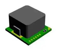
MUN20AD03-SM
DC-DC Converter, Non-Isolated, Micro Module, Adjustable, 9V to 24V, 3A
⚠️ Reference pricing provided. In case of supply shortages, we will connect you with our trusted procurement partners to ensure your project's continuity.
- Manufacturer: CYNTEC
- Product type: DC / DC Non Isolated Board Mount Converters - Adjustable Output
- SVHC: No SVHC (21-Jan-2025)
- Depth: 6mm
- Width: 6mm
- Height: 3.5mm
- Product Range: -
- Output Power Max: 16.5W
- Output Current Max: 3A
- Output Voltage Max: 5.5V
- Output Voltage Min: 600mV
- Input Voltage DC Max: 24V
- Input Voltage DC Min: 9V
- DC / DC Converter Type: Micro Module
- Power Supply Applications: Communications Equipment, Networking Equipment, Servers and Storage Equipments
- DC / DC Converter Output Type: Adjustable
| Delivery and price | |
|---|---|
| Units per pack | 500 |
| Price | 4.69 € |
| Current stock | 1000+ |
| Lead time | 30 days |
Datasheet

**MUN20AD03-SM**

## **uPOL Module**

## **3A, High Efficiency uPOL Module**

- **GENERAL DESCRIPTION:**

- **FEATURES:**

- ~~ee FO~~ ◼ High Density uPOL Module The uPOL module is non-isolated dc-dc

- ◼ 3A Output Current

The uPOL module is non-isolated dc-dc converters that can deliver up to 3A of output current. The PWM switching regulator, high frequency power inductor are integrated in one hybrid package. The module has automatic operation with PWM mode and power saving mode according to loading. Instant PWM architecture to achieve fast transient responses. Other features include remote enable function, internal soft-start, non-latching over current protection and power good.

- Input Voltage Range from 9V to 24V

- Output Voltage Range from 0.6V to 5.5V

- 93% Peak Efficiency(@Vin=20V)

- Enable / PGOOD Function

- Automatic Power Saving/PWM Mode

- Protections (OCP, OTP, SCP, OVP: Non-latching )

- Internal Soft Start

- Compact Size: 6mm*6mm*3.5mm(Max)

- Pb-free for RoHS compliant

- MSL 2, 250C Reflow

The low profile and compact size package (6.0mm × 6.0mm x 3.5mm) is suitable for automated assembly by standard surface mount equipment. The uPOL module is Pb-free and RoHS compliance.

> **APPLICATIONS:** [Po ◼ Distributed Power Supply

- Server, Workstation, and Storage

- ◼ Networking and Datacom

## **TYPICAL APPLICATION CIRCUIT:** ~~See~~

VBIAS

**==> picture [250 x 113] intentionally omitted <==**

**----- Start of picture text -----**<br>
VPGOOD  RPGood<br>PGOOD  FB  CFB1  RFB1<br>VIN<br>VOUT<br>VIN<br>MUN20AD03-SM<br>CIN  COUT<br>EN  RFB2<br>Vcc  GND  ILIM<br>C1<br>**----- End of picture text -----**<br>


**FIGURE. 1 TYPICAL APPLICATION CIRCUIT**

**FIGURE. 2 HIGH DENSITY uPOL MODULE**

1

Rev.A1

## **MUN20AD03-SM**

## **ORDER INFORMATION:**

||**Ambient Temp. Range**|**Package**|||
|---|---|---|---|---|
|**Part Number**|||**MSL**|**Note**|
||**(°C)**|**(Pb-Free)**|||
|MUN20AD03-SM|-40 ~ +85|QFN|Level 2|-|
||||||
|**Order Code**||**Packing**||**Quantity**|
|MUN20AD03-SM||Tape and reel||1000|


## **PIN CONFIGURATION:**

**==> picture [388 x 384] intentionally omitted <==**

**----- Start of picture text -----**<br>
LI LJ LI LI Ld<br>VW rT FT fa. ord<br>VIN_TPD(21)<br>VIN(1)  (15)ILIM<br>ee _ =<br>[<br>PHASE_TPD<br>PHASE(2)  (14)VOUT<br>(22)<br>ee ee ee<br>en ee<br>PHASE(3)  (13)VOUT<br>GND_TPD<br>(23)<br>PHASE(4)  (12)VOUT<br>L_] L_]<br>GND(5)  LJ | | | LJ (11)VOUT<br>rT oF. fa. rd<br>LI LJ LI LI Ld<br>(20)VIN  (19)VIN  (18)BST  (17)VCC  (16)FB<br>(25)<br>GND_TPD<br>(24)<br>VOUT_TPD<br>GND(6)  GND(7)  EN(8)<br>PGOOD(9)  VOUT(10)<br>**----- End of picture text -----**<br>


**TOP VIEW**

2

Rev.A1

**MUN20AD03-SM**

> **PIN DESCRIPTION:** ~~TT~~

|**Symbol**|**Pin No.**|**Description**|
|---|---|---|
|VIN|1, 19, 20|Power input pin. It needs to connect input rail and thermal exposed pad<br>of VIN_TPD(21) for heat transferring. Place the input ceramic type<br>capacitor as closely as possible to this pin. One capacitor of 10uF at least<br>for input capacitance.|
|PHASE|2, 3, 4|Switch output. Connect to thermal exposed pad of PHASE_TPD(22) for<br>heat transferring.|
|GND|5, 6, 7|Power ground pin for signal, input, and output return path. This pin<br>needs to connect one or more ground plane directly. Connect to thermal<br>exposedpad of GND_TPD(23,25)for heat transferring.|
|EN|8|On/Off control pin for module.|
|PGOOD|9|Power good signal pin. Open drain output when the output voltage is<br>within 90% to 120% of regulationpoint.|
|VOUT|10, 11, 12,<br>13, 14|Power output pin. Connect to output and thermal exposed pad of<br>VOUT_TPD(24) for heat transferring. Place the output capacitors as<br>closelyaspossible to thispin.|
|ILIM|15|Current limit setting pin. Connect to GND for current limit setting.|
|FB|16|Feedback input. Connect an external resistor divider from the VOUT to<br>FB toprogram the output voltage.|
|VCC|17|Internal 3.3V LDO output. Power supply for internal analog circuits and<br>drivingcircuit. Connect a 2.2uF for Bypass capacitor.|
|BST|18|Boot-Strap Pin. No need connect.|
|VIN_TPD|21|Power input pin. Connect input rail and using for heat transferring to heat<br>dissipation layer byVias connection.|
|PHASE_TPD|22|Phase node pin. Using for heat transferring to heat dissipation layer by<br>Vias connection.|
|GND_TPD|23, 25|Power ground pin. It needs to connect one or more ground plane directly<br>and using for heat transferring to heat dissipation layer by Vias<br>connection.|
|VOUT_TPD|24|Power output pin. Connect to output and using for heat transferring to<br>heat dissipation layer byVias connection.|


3

Rev.A1

**MUN20AD03-SM**

## **ELECTRICAL SPECIFICATIONS:** ~~TT~~

CAUTION: Do not operate at or near absolute maximum rating listed for extended periods of time. This stress may adversely impact product reliability and result in failures not covered by warranty.

|**Parameter**<br>~~ee~~|**Description**|**Min.**|**Typ.**|**Max.**|**Unit**|
|---|---|---|---|---|---|
|◼<br>Absolute Maximum Ratings<br>~~ee~~<br>~~ee~~<br>~~es~~||||||
|VIN to GND<br>~~es~~<br>~~ee~~|~~ee~~|-|-|+30.0|V|
|VOUT to GND<br>~~es~~<br>~~ee~~<br>~~ee~~|~~ee~~|-|-|+6.0|V|
|PHASE to GND<br>~~ee ~~<br>~~ee~~<br>~~es~~|~~ee~~|||+30.0|V|
|PGOOD to GND<br>~~ee~~<br>~~es~~<br>~~es~~|~~es~~|~~es~~|~~es~~|+30.0<br>~~es~~|V<br>~~es~~|
|ILIM to GND<br>~~es~~<br>~~es~~<br>~~es~~|~~es~~<br>~~es~~|~~es~~<br>~~es~~|~~es~~<br>~~es~~|+4.0<br>~~es~~<br>~~es~~|V<br>~~es~~<br>~~es~~|
|VCC to GND<br>~~es~~<br>~~es~~<br>~~es~~|~~es~~<br>~~es~~<br>~~es~~|~~es~~<br>~~es~~<br>~~es~~|~~es~~<br>~~es~~<br>~~es~~|+4.0<br>~~es~~<br>~~es~~<br>~~es~~|V<br>~~es~~<br>~~es~~<br>~~es~~|
|FB to GND<br>~~es~~<br>~~es~~<br>~~ee~~|~~es~~<br>~~es~~<br>~~ee~~|~~es~~<br>~~es~~<br>~~ee~~|~~es~~<br>~~es~~<br>~~ee~~|+4.0<br>~~es~~<br>~~es~~<br>~~ee~~|V<br>~~es~~<br>~~es~~<br>~~ee~~|
|EN to GND<br>~~es~~<br>~~ee~~<br>~~es~~|~~es~~<br>~~ee~~|-<br>~~es~~<br>~~ee~~|-<br>~~es~~<br>~~ee~~|+30.0<br>~~es~~<br>~~ee~~|V<br>~~es~~<br>~~ee~~|
|Tc<br>~~ee~~<br>~~es~~<br>~~es~~|Case Temperature of Inductor<br>~~ee~~<br>~~es~~|-<br>~~ee~~<br>~~es~~<br>~~ss~~|-<br>~~ee~~<br>~~es~~<br>~~ss~~|+110<br>~~ee~~<br>~~es~~|°C<br>~~ee~~<br>~~es~~|
|Tstg<br>~~es~~<br>~~es~~|Storage Temperature<br>~~es~~|-40<br>~~es~~<br>~~ss~~|-<br>~~es~~<br>~~ss~~|+125<br>~~es~~|°C<br>~~es~~|
|◼<br>Recommendation Operating Ratings<br>~~eses~~<br>~~ss~~<br>~~|~~<br>~~esee~~||||||
|VIN<br>~~es~~<br>~~ee~~|Input Supply Voltage<br>~~ee~~<br>~~ee~~|+9<br>~~ee~~|-<br>~~ee~~|+24<br>~~ee~~|V<br>~~ee~~|
|VOUT<br>~~es~~<br>~~ee~~<br>~~ee~~|Adjusted Output Voltage<br>~~ee~~<br>~~ee~~<br>~~es~~|+0.6<br>~~ee~~<br>~~es~~|~~ee~~<br>~~es~~|+5.5<br>~~ee~~<br>~~es~~|V<br>~~ee~~<br>~~es~~|
|Ta<br>~~ee~~<br>~~ee~~<br>~~ee~~|Ambient Temperature<br>~~ee~~<br>~~es~~|-40<br>~~ee~~<br>~~es~~|-<br>~~ee~~<br>~~es~~|+85<br>~~ee~~<br>~~es~~|°C<br>~~ee~~<br>~~es~~|
|◼<br>Thermal Information<br>~~eees~~<br>~~ee~~||||||
|Rth(jchoke-a)<br>~~ee~~|Thermal resistance from junction to<br>ambient(Note 1)|-|21.7|-|°C/W|


NOTES:

1. Rth(jchoke-a) is measured with the component mounted on an effective thermal conductivity test board on 0 LFM condition. The test board size is 30mm× 30mm× 1.6mm with 4 layers. The test condition is complied with JEDEC EIJ/JESD 51 Standards.

4

Rev.A1

**MUN20AD03-SM**

## ee **ELECTRICAL SPECIFICATIONS: (Cont.)**

Conditions: TA = 25 ºC, unless otherwise specified. Test Board Information: 30mm× 30mm× 1.6mm, 4 layers 2 Oz. The output ripple and transient response measurement is short loop probing and 20MHz bandwidth limited. Vin=20V Vout= 5V Cin = 10uF/25V 1206 × 2, Cout = 47uF/6.3V/ 1206x3

|~~a~~|~~ee~~|~~es~~|~~es~~|~~es~~|~~es~~||
|---|---|---|---|---|---|---|
|**Symbol**<br>~~a~~|**Parameter**<br>~~ee~~|**Conditions**<br>~~es~~|**Min.**<br>~~es~~|**Typ.**<br>~~es~~|**Max.**<br>~~es~~|**Unit**|
|◼<br>Input Characteristics<br>~~a~~<br>~~ee~~<br>~~es es es es~~<br>~~ee~~<br>~~a~~<br>~~ee ee~~|||||||
|ISD(IN)<br>~~a~~<br>~~a~~|Input shutdown current<br>~~ee ee~~<br>~~es ee~~|Vin =20V, EN = GND<br>~~ee~~<br>~~ee~~|-<br>~~Ge~~|10<br>~~Ge~~|-<br>~~ee~~|uA|
|I(IN)<br>~~a~~<br>~~a~~|Input supply current<br>~~ee ee~~<br>~~es ee~~|Vin = 20V, Iout = 0A<br>Vout = 5V,EN = 5V<br>~~ee~~<br>~~ee~~|-<br>~~Ge~~<br>~~ns~~|100<br>~~Ge~~|-<br>~~ee~~|uA|
|IS(IN)<br>~~a ~~<br>~~i~~|Input supply current<br> ~~es ee~~<br>~~i~~|Vin = 20V,EN = Vin<br>~~ee~~<br>~~es~~<br>~~i~~|~~Ge~~<br>~~es~~<br>~~ns~~<br>~~i~~|~~Ge~~<br>~~es~~<br>~~i~~|~~ee~~<br>~~es~~<br>~~i~~|~~es~~<br>~~i~~|
|||Iout = 5mA,Vout =5V<br>~~i~~|-<br>~~ns~~<br>~~i~~|2<br>~~i~~|-<br>~~i~~|mA<br>~~i~~|
|||Iout = 3A,Vout =5V<br>~~i~~|-<br>~~i~~|1<br>~~i~~|-<br>~~i~~|A<br>~~i~~|
|◼<br>Output Characteristics<br>~~ee~~<br>~~a~~<br>~~eeGe~~~~**s**~~<br>~~ese~~<br>~~es~~|||||||
|IOUT(DC)<br>~~ee~~<br>~~a~~|Output continuous<br>current range<br>~~ee~~<br>~~ee~~|~~ee~~<br>~~Ge~~<br>~~ee~~|0<br>~~ee~~<br>~~Ge~~<br>~~es~~|-<br>~~ee~~<br>~~Ge~~~~**s**~~<br>~~e~~<br>~~ee~~|3<br>~~ee~~<br>~~**s**~~<br>~~es~~<br>~~ee~~|A<br>~~ee~~<br>~~**s**~~<br>~~ee~~|
|VO(SET)<br>~~a~~<br>~~ee~~<br>~~a~~|Ouput Voltage Set Point<br>~~ee~~<br>~~ee~~|With 0.1% tolerance for<br>external resistor used to set<br>output voltage<br>~~Ge~~<br>~~ee~~<br>~~ee~~<br>~~ee~~|-3<br>~~Ge~~<br>~~es ~~<br>~~ee~~<br>~~e~~|~~Ge~~~~**s**~~<br> ~~e~~<br>~~ee~~<br>~~ee~~<br>~~e~~~~**e**~~|+3<br>~~**s**~~<br>~~es~~<br>~~ee~~<br>~~ee~~<br>~~**e**e~~|% VO(SET)<br>~~**s**~~<br>~~ee~~<br>~~ee~~<br>~~e~~|
|ΔVOUT/ΔVIN<br>~~ee~~<br>~~a~~|Line regulation accuracy<br>~~ee~~<br>~~ee~~|Vin = 12 to 20V<br>Vout = 5V, Iout = 0A<br>Vout = 5V,Iout = 3A<br>~~ee~~<br>~~ee~~<br>~~ee~~<br>~~ee~~|-<br>~~ee~~<br>~~e~~<br>~~Ge~~|2<br>~~ee~~<br>~~ee~~<br>~~e~~~~**e**~~<br>~~e~~|~~ee~~<br>~~ee~~<br>~~**e**e~~<br>~~es~~|% VO(SET)<br>~~ee~~<br>~~ee~~<br>~~e~~|
|ΔVOUT/ΔIOUT<br>~~a~~|OUT<br>Load regulation accuracy<br>~~ee~~|Iout = 0A to 3A<br>Vin = 20V,Vout = 5V<br>~~ee ~~<br>~~ee~~<br>~~——~~|-4<br> ~~e~~<br>~~Ge~~|~~e~~~~**e**~~<br>~~e~~|+3<br>~~**e**e~~<br>~~es~~|% VO(SET)<br>~~e~~|
|VOUT(AC)<br>~~a~~|Output ripple voltage<br>~~ee~~<br>~~a~~|Vin = 20V, Vout = 5V<br>EN = Vin,20MHz Bandwidth<br>~~ee ~~<br>~~a~~<br>~~——~~|-<br> ~~Ge~~<br>~~a~~|-<br>~~e~~<br>~~a~~|-<br>~~es~~<br>~~a~~|-<br>~~a~~|
|||IOUT = 5mA<br>~~a~~<br>~~——~~|~~a~~<br>~~ED~~|50<br>~~a~~<br>~~I~~|~~a~~|mVp-p<br>~~a~~|
|||IOUT = 3A<br>~~a~~<br>~~——~~<br>~~ns~~|~~a~~<br>~~ns~~<br>~~ED~~|20<br>~~a~~<br>~~ns~~<br>~~I~~|~~a~~<br>~~ns~~|mVp-p<br>~~a~~<br>~~ns~~|
|◼<br>Dynamic Characteristics<br>~~——~~<br>~~ED I~~<br>~~Pe~~<br>~~e~~<br>~~ee~~|||||||
|ΔVOUT-DP<br>~~e~~|Voltage change for<br>positive load step<br>~~e~~|Iout = 1.5A to 3A<br>Current slew rate = 0.15A/uS<br>Vin = 20V,Vout = 5V<br>~~e~~~~**e**~~<br>~~e~~<br>~~ee~~|Current slew rate = 0.15A/uS<br>-<br>~~**e**~~<br>~~eee~~|30<br>~~**e**~~<br>~~ee~~<br>~~eee~~|-<br>~~**e**~~<br>~~ee~~<br>~~eee~~|mVp-p<br>~~**e**~~<br>~~ee~~<br>~~eee~~|
|ΔVOUT-DN<br>~~ee~~|Voltage change for<br>negative load step<br>~~ee~~|Iout = 3A to 1.5A<br>Current slew rate = 0.15A/uS<br>Vin = 20V,Vout = 5V<br>~~e~~<br>~~ee~~<br>~~ee~~|Current slew rate = 0.15A/uS<br>-<br>~~ee~~<br>~~eee~~|30<br>~~ee~~<br>~~ee~~<br>~~eee~~|-<br>~~ee~~<br>~~ee~~<br>~~eee~~|mVp-p<br>~~ee~~<br>~~ee~~<br>~~eee~~|
|◼<br>Control Characteristics<br>~~ee eee~~<br>~~eee~~|||||||
|FOSC<br>~~a er~~<br>~~ee~~|Oscillator frequency<br>~~er~~<br>~~es eer~~|PWM Mode<br>~~er~~<br>~~eer~~|~~er~~<br>~~nn~~|0.8<br>~~er~~<br>~~nn~~|~~er~~<br>~~nn~~|MHz<br>~~er~~|
|VREF<br>~~ee~~<br>~~a~~|Referance voltage<br>~~es eer~~<br>~~ee~~|PWM Mode<br>~~eer~~<br>~~tes Gt~~|0.594<br>~~nn~~<br>~~Gt~~|0.600<br>~~nn~~<br>~~Gs ee~~|0.606<br>~~nn~~<br>~~ee~~|V|
|VPG<br>~~ee~~<br>~~a~~<br>~~a~~|Power good threshold<br>~~es eer~~<br>~~ee~~<br>~~ee Mere~~|VFBRising<br>~~eer~~<br>~~tes Gt~~<br>~~Mere~~|88<br>~~nn~~<br>~~Gt~~<br>~~ttt~~|90<br>~~nn~~<br>~~Gs ee~~<br>~~en~~|92<br>~~nn~~<br>~~ee~~<br>~~en~~|% VREF|
|VPGL<br>~~a~~<br>~~a~~<br>~~a~~|Power good Low<br>~~ee~~<br>~~ee Mere~~<br>~~re ee~~|IPOOD=4mA<br>~~tes Gt~~<br>~~Mere~~<br>~~ee~~|0.04<br>~~Gt ~~<br>~~ttt~~|0.15<br> ~~Gs ee~~<br>~~en~~|0.3<br>~~ee~~<br>~~en~~|V|
|IILIM<br>~~a~~<br>~~a~~<br>~~a~~|Over current limit<br>~~ee Mere~~<br>~~re ee~~<br>~~rs~~|ILIM=GND<br>~~Mere~~<br>~~ee~~|4<br>~~ttt~~|~~en~~|8<br>~~en~~|A|
|VENL<br>~~a~~<br>~~a~~<br>~~ee~~|EN Low threshold<br>~~re ee~~<br>~~rs~~<br>~~es eer~~|~~ee~~<br>~~eer~~|-<br>~~nn~~|-<br>~~nn~~|0.3<br>~~nn~~|V|
|VENH<br>~~a~~<br>~~ee~~<br>~~ee~~|EN High Threshold<br>~~rs~~<br>~~es eer~~<br>~~er~~|~~eer~~<br>~~er~~|0.85<br>~~nn~~<br>~~er~~|-<br>~~nn~~<br>~~er~~|VIN<br>~~nn~~<br>~~er~~|V<br>~~er~~|
|TSS<br>~~ee~~<br>~~ee~~<br>~~ae~~|Soft Start Time<br>~~es eer~~<br>~~er~~<br>~~ee~~|~~eer~~<br>~~er~~<br>~~es~~|~~nn~~<br>~~er~~<br>~~es~~|600<br>~~nn~~<br>~~er~~<br>~~es~~|~~nn~~<br>~~er~~<br>~~ee~~|uS<br>~~er~~|
|Eff<br>~~ee~~<br>~~ae~~|Efficinecy<br>~~er~~<br>~~ee~~|VIN=20V ,VOUT=5V<br>IOUT=3A<br>~~er~~<br>~~es~~|~~er~~<br>~~es~~|93<br>~~er~~<br>~~es~~|~~er~~<br>~~ee~~|%<br>~~er~~|


5

Rev.A1

**MUN20AD03-SM**

## **TYPICAL PERFORMANCE CHARACTERISTICS: (5.0VOUT)**

Conditions: TA = 25 ºC, unless otherwise specified. Test Board Information: 30mm× 30mm× 1.6mm, 4 layers 2 Oz. The output ripple and transient response measurement is short loop probing and 20MHz bandwidth limited. Cin = 10uF/25V 1206 × 2, Cout = 47uF/6.3V/ 1206x3

The following figures provide the typical characteristic curves at 5.0Vout.

**==> picture [405 x 363] intentionally omitted <==**

**----- Start of picture text -----**<br>
FIG.3 EFFICIENCY V.S. LOAD CURRENT  FIG.4 24VIN DE-RATING CURVE<br>Stop r ek Stop |<br>SY 500KS/s @.- 2.50GS/s @r<br>——__di0.000005ioomves 100k points _3.40mv (@divio0omvys 0.000005 100K points _10.2mv<br>value Mean Min Max Std Dev 10:52:17 Value Mean Min Max Std Dev<br>@Peak-Peak 44.0mV 45.7m 44.0m 49.2m 2.14m @ Peak-Peak 21.2mV_—21.2m 21.2m 21.2m 0.00<br>FIG.5 OUTPUT RIPPLE  FIG.6 OUTPUT RIPPLE<br>(20VIN, 5.0VOUT, IOUT=0A)  (20VIN, 5.0VOUT, IOUT=3A)<br>Stop j Tek Stop i<br>EN<br>4) Vout<br>H iD<br>PGOOD<br>a0US 25.0MS/s Dr tiaratritide iaearrireic ibaricai eateries<br>ii+y-6.00000ys 100k points 2.28A<br>value Mean Min Max Std Dev<br>@Peak-Peak 30.82mV 31.02m  —30.65m = 31.63m = 338.9 @20v 4 @ 100ys 100MS/s @ F<br>@ max 15.51mV 15.92m —-15.51m_ —16.58m 362.81 09:28:06 @ 5.00V % iivv0.00000s 100k points 4.72<br>@uin =15.31mV_-15.10m _-15.57m __-14.81m__238.8 V<br>FIG.7   TRANSIENT RESPONSE  FIG.8  TURN-ON<br>(20VIN, 5.0VOUT, 50% to 100% LOAD STEP) (20VIN, 5.0VOUT, IOUT=3A)<br>**----- End of picture text -----**<br>


6

Rev.A1

**MUN20AD03-SM**

> **APPLICATIONS INFORMATION:** ~~ee~~

## **REFERENCE CIRCUIT FOR GENERAL APPLICATION:**

Figure 9 shows the module application schematics for input voltage +20V and turn on by input voltage directly through enable resistor (REN).

**==> picture [421 x 142] intentionally omitted <==**

**----- Start of picture text -----**<br>
R1  VBIAS<br>100k<br>RFB1  150pF CFB<br>Input Voltage  PGOOD  FB<br>20V  Output Voltage<br>VIN  VOUT<br>MUN20AD03-SM<br>C1  C2<br>10uF  10uF  EN  RFB2  47uFX3 C4,5,6  100nF C7<br>C3  T Vcc  GND  ILIM  e<br>2.2uF<br>**----- End of picture text -----**<br>


## **FIG.9 REFERENCE CIRCUIT FOR GENERAL APPLICATION**

7

Rev.A1

## **MUN20AD03-SM**

## **APPLICATIONS INFORMATION: (Cont.)**

## **INPUT FILTERING:**

The module should be connected to a source supply of low AC impedance and high inductance in which line inductance can affect the module stability. An input capacitor must be placed as near as possible to the input pin of the module so to minimize input ripple voltage and ensure module stability.

## **OUTPUT FILTERING:**

To reduce output ripple and improve the dynamic response as the step load changes, an additional capacitor at the output must be connected. Low ESR polymer and ceramic capacitors are recommended to improve the output ripple and dynamic response of the module.

## **PROGRAMMING OUTPUT VOLTAGE:**

The module has an internal 0.6V ± 1.1% reference voltage. The output voltage can be programmed by the dividing resistor (RFB) which connects to both Vout pin and FB pin. The output voltage can be calculated by Equation 1, resistor choice may be referred TABLE 1.

**==> picture [307 x 37] intentionally omitted <==**

|Vout|RFB1(Ohm)|RFB2 (Ohm)|
|---|---|---|
|1.0V|13.3k|20k|
|1.2V|20.0k|20k|
|1.8V|40.2k|20k|
|2.5V|63.3k|20k|
|3.3V|90.8k|20k|
|5.0V|147k|20k|


**TABLE 1 Resistor values for common output voltages**

8

Rev.A1

**MUN20AD03-SM**

## **REFLOW PARAMETERS:** ~~a~~

Lead-free soldering process is a standard of electronic products production. Solder alloys like Sn/Ag, Sn/Ag/Cu and Sn/Ag/Bi are used extensively to replace the traditional Sn/Pb alloy. Sn/Ag/Cu alloy (SAC) is recommended for this power module process. In the SAC alloy series, SAC305 is a very popular solder alloy containing 3% Ag and 0.5% Cu and easy to obtain. Figure 56 shows an example of the reflow profile diagram. Typically, the profile has three stages. During the initial stage from room temperature to 150°C, the ramp rate of temperature should not be more than 3°C/sec. The soak zone then occurs from 150°C to 200°C and should last for 60 to 120 seconds. Finally, keep at over 217°C for 60~150 seconds to melt the solder and make the peak temperature at the range from 245°C to 250°C (Do not exceed 30 sec). It is noted that the time of peak temperature should depend on the mass of the PCB board. The reflow profile is usually supported by the solder vendor and one should adopt it for optimization according to various solder type and various manufacturers’ formulae.

**FIG.10 Recommendation Reflow Profile**

## **(Not to scale)**

***Refer to the Classification Reflow Profile of J-STD-020.**

9

Rev.A1

**MUN20AD03-SM**

## **APPLICATIONS INFORMATION: (Cont.)**

## **Recommendation Layout Guide:**

In order to achieve stable, low losses, less noise or spike, and good thermal performance some layout considerations are necessary. The recommendation layout is shown as Figure 59-62.

1. The ground connection between pin 23, pin25 and pin 5 to 7 should be a solid ground plane under the module. It can be connected one or more ground plane by using several Vias

2. Place high frequency ceramic capacitors between pin 1, pin 19 to 21 (VIN), and pin 23, pin25, pin 5 to 7 (GND) for input side; and pin 24, pin 10 to 14 (VOUT), and pin 23, pin25, pin 5 to 7 (GND) for output side, as close to module as possible to minimize high frequency noise.

3. Keep the RFB connection trace to the module pin 16 (FB) short.

4. Use large copper area for power path (VIN, VOUT, and GND) to minimize the conduction loss and enhance heat transferring. Also, use multiple Vias to connect power planes in different layer.

5. Avoid any sensitive signal traces near the pin 24, and pin 2 to 4 (PHASE).

**FIG.11 Recommendation Layout (Top)**

10

Rev.A1

**MUN20AD03-SM**

- **FIG.12 Recommendation Layout (Middle 1)**

- ai

**FIG.13 Recommendation Layout (Middle 1)**

11

Rev.A1

**MUN20AD03-SM**

**FIG.14 Recommendation Layout (Middle 1)**

## **THERMAL CONSIDERATIONS:**

All of thermal testing condition is complied with JEDEC EIJ/JESD 51 Standards. Therefore, the test board size is 30mm× 30mm× 1.6mm with 4 layers 2oz. The case temperature of module sensing point is shown as FIG.15 Then Rth(jchoke-a) is measured with the component mounted on an effective thermal conductivity test board on 0 LFM condition. The module is designed for using when the case temperature is below 110°C regardless the change of output current, input/output voltage or ambient temperature.

## **Sensing point (Defined case temperature)**

**FIG.15 CASE TEMPERATURE SENSING POINT**

12

Rev.A1

**MUN20AD03-SM**

## **PACKAGE OUTLINE DRAWING:**

Unit: mm General Tolerance: +/- 0.1mm

13

Rev.A1

## **MUN20AD03-SM**

## **LAND PATTERN REFERENCE:**

**==> picture [49 x 9] intentionally omitted <==**

**----- Start of picture text -----**<br>
Unit: mm<br>**----- End of picture text -----**<br>


*Based on 0.1~0.15mm thickness stencil (Reference only)

*Recommended solder paste coverage 55~100%

14

Rev.A1

## **MUN20AD03-SM**

**==> picture [461 x 14] intentionally omitted <==**

**----- Start of picture text -----**<br>
  PACKING REFERENCE:  Lt<br>**----- End of picture text -----**<br>


|Unit: mm<br>4<br>~~a~~|Unit: mm<br>4<br>~~a~~|Unit: mm<br>4<br>~~a~~|Unit: mm<br>4<br>~~a~~|Unit: mm<br>4<br>~~a~~|Unit: mm<br>4<br>~~a~~|||D<br>~~NN~~|D<br>~~NN~~|D<br>~~NN~~||||**Package In Tape Loading Orientation**<br>**Tape Dimension**<br>pulling direction<br>Sprocket Hole<br>— Pin 1 Mark<br>et<br>P~~l~~<br>~~PO~~<br>~~P2~~<br>~~a~~<br>~~di~~<br>~~Le~~<br>2<br>|<br>~~|~~<br>So<br>~~A~~O|**Package In Tape Loading Orientation**<br>**Tape Dimension**<br>pulling direction<br>Sprocket Hole<br>— Pin 1 Mark<br>et<br>P~~l~~<br>~~PO~~<br>~~P2~~<br>~~a~~<br>~~di~~<br>~~Le~~<br>2<br>|<br>~~|~~<br>So<br>~~A~~O|**Package In Tape Loading Orientation**<br>**Tape Dimension**<br>pulling direction<br>Sprocket Hole<br>— Pin 1 Mark<br>et<br>P~~l~~<br>~~PO~~<br>~~P2~~<br>~~a~~<br>~~di~~<br>~~Le~~<br>2<br>|<br>~~|~~<br>So<br>~~A~~O|**Package In Tape Loading Orientation**<br>**Tape Dimension**<br>pulling direction<br>Sprocket Hole<br>— Pin 1 Mark<br>et<br>P~~l~~<br>~~PO~~<br>~~P2~~<br>~~a~~<br>~~di~~<br>~~Le~~<br>2<br>|<br>~~|~~<br>So<br>~~A~~O|**Package In Tape Loading Orientation**<br>**Tape Dimension**<br>pulling direction<br>Sprocket Hole<br>— Pin 1 Mark<br>et<br>P~~l~~<br>~~PO~~<br>~~P2~~<br>~~a~~<br>~~di~~<br>~~Le~~<br>2<br>|<br>~~|~~<br>So<br>~~A~~O|**Package In Tape Loading Orientation**<br>**Tape Dimension**<br>pulling direction<br>Sprocket Hole<br>— Pin 1 Mark<br>et<br>P~~l~~<br>~~PO~~<br>~~P2~~<br>~~a~~<br>~~di~~<br>~~Le~~<br>2<br>|<br>~~|~~<br>So<br>~~A~~O|**Package In Tape Loading Orientation**<br>**Tape Dimension**<br>pulling direction<br>Sprocket Hole<br>— Pin 1 Mark<br>et<br>P~~l~~<br>~~PO~~<br>~~P2~~<br>~~a~~<br>~~di~~<br>~~Le~~<br>2<br>|<br>~~|~~<br>So<br>~~A~~O|**Package In Tape Loading Orientation**<br>**Tape Dimension**<br>pulling direction<br>Sprocket Hole<br>— Pin 1 Mark<br>et<br>P~~l~~<br>~~PO~~<br>~~P2~~<br>~~a~~<br>~~di~~<br>~~Le~~<br>2<br>|<br>~~|~~<br>So<br>~~A~~O|**Package In Tape Loading Orientation**<br>**Tape Dimension**<br>pulling direction<br>Sprocket Hole<br>— Pin 1 Mark<br>et<br>P~~l~~<br>~~PO~~<br>~~P2~~<br>~~a~~<br>~~di~~<br>~~Le~~<br>2<br>|<br>~~|~~<br>So<br>~~A~~O|**Package In Tape Loading Orientation**<br>**Tape Dimension**<br>pulling direction<br>Sprocket Hole<br>— Pin 1 Mark<br>et<br>P~~l~~<br>~~PO~~<br>~~P2~~<br>~~a~~<br>~~di~~<br>~~Le~~<br>2<br>|<br>~~|~~<br>So<br>~~A~~O|**Package In Tape Loading Orientation**<br>**Tape Dimension**<br>pulling direction<br>Sprocket Hole<br>— Pin 1 Mark<br>et<br>P~~l~~<br>~~PO~~<br>~~P2~~<br>~~a~~<br>~~di~~<br>~~Le~~<br>2<br>|<br>~~|~~<br>So<br>~~A~~O|**Package In Tape Loading Orientation**<br>**Tape Dimension**<br>pulling direction<br>Sprocket Hole<br>— Pin 1 Mark<br>et<br>P~~l~~<br>~~PO~~<br>~~P2~~<br>~~a~~<br>~~di~~<br>~~Le~~<br>2<br>|<br>~~|~~<br>So<br>~~A~~O|**Package In Tape Loading Orientation**<br>**Tape Dimension**<br>pulling direction<br>Sprocket Hole<br>— Pin 1 Mark<br>et<br>P~~l~~<br>~~PO~~<br>~~P2~~<br>~~a~~<br>~~di~~<br>~~Le~~<br>2<br>|<br>~~|~~<br>So<br>~~A~~O|**Package In Tape Loading Orientation**<br>**Tape Dimension**<br>pulling direction<br>Sprocket Hole<br>— Pin 1 Mark<br>et<br>P~~l~~<br>~~PO~~<br>~~P2~~<br>~~a~~<br>~~di~~<br>~~Le~~<br>2<br>|<br>~~|~~<br>So<br>~~A~~O|**Package In Tape Loading Orientation**<br>**Tape Dimension**<br>pulling direction<br>Sprocket Hole<br>— Pin 1 Mark<br>et<br>P~~l~~<br>~~PO~~<br>~~P2~~<br>~~a~~<br>~~di~~<br>~~Le~~<br>2<br>|<br>~~|~~<br>So<br>~~A~~O|**Package In Tape Loading Orientation**<br>**Tape Dimension**<br>pulling direction<br>Sprocket Hole<br>— Pin 1 Mark<br>et<br>P~~l~~<br>~~PO~~<br>~~P2~~<br>~~a~~<br>~~di~~<br>~~Le~~<br>2<br>|<br>~~|~~<br>So<br>~~A~~O|**Package In Tape Loading Orientation**<br>**Tape Dimension**<br>pulling direction<br>Sprocket Hole<br>— Pin 1 Mark<br>et<br>P~~l~~<br>~~PO~~<br>~~P2~~<br>~~a~~<br>~~di~~<br>~~Le~~<br>2<br>|<br>~~|~~<br>So<br>~~A~~O|pulling direction|
|---|---|---|---|---|---|---|---|---|---|---|---|---|---|---|---|---|---|---|---|---|---|---|---|---|---|---|---|---|---|---|---|
|||||||||||||||||||||||||||||||||
|||||||||||A0||A0||||6.60±0.10||E1|||||||1.75||||1.75±|±0.10||
|||||||||||B0||B0||||6.60±0.10||K0|||||||3.70||||3.70±|±0.10||
|||||||||||F||||||7.50±0.10||P0|||||||12.00±|||||±0.10||
|||||||||||W||||||16.00±0.30||P1|||||||2.00||||2.00±|±0.10||
|||||||||||D0||D0||||φ1.5 +0.1/-0.0||P2|||||||4.00||||4.00±|±0.10||
|||||||||||D1||D1||||φ1.5 Min.||t|t||||||0.35||||0.35±|±0.05||


15

Rev.A1

# **MUN20AD03-SM**

> **PACKING REFERENCE: (Cont.)** ~~LT~~

**==> picture [322 x 319] intentionally omitted <==**

**----- Start of picture text -----**<br>
Unit: mm<br>Reel Dimension<br>See Detail A<br>( XD<br>Nas<br>=<br>Peel Strength of Top Cover Tape<br>The peel speed shall be about 300mm/min.<br>**----- End of picture text -----**<br>


**==> picture [31 x 6] intentionally omitted <==**

**----- Start of picture text -----**<br>
Detail A<br>**----- End of picture text -----**<br>


The peel force of top cover tape shall between 0.1N to 1.3N

16

Rev.A1

**MUN20AD03-SM**

> **REVERSION HISTORY:** ~~TT~~

|**Date**|**Revision**|**Changes**|
|---|---|---|
|2015.10.29|Preliminary|Release the preliminary specification.|
|2016.05.05|01|Change FB Resistor for output voltages|
|2016.06.19|02|Add test Conditions<br>Change Recommendation Operating Ratings|
|2017.03.30|03|Add PGOOD sink current spec|
|2022.12.23|04|1.<br>Page 9 update reflow parameters and FIG.10<br>2.<br>Page 12, Add “THERMAL CONSIDERATIONS”.<br>3.<br>Page 14 change the thickness description of stencil. Add<br>note.|
|2024.12.16|A1|Synchronized with document management number|


17

Rev.A1
Updated at June 9, 2026
About Novapart
Novapart is a B2B electronic component broker specialising in stock shortages and cost reduction. We source hard-to-find parts and identify compliant alternatives across a catalogue of 410,000+ components from 500+ manufacturers.
Learn more →Stock Shortage Specialist
When a component is unavailable, discontinued or has an unacceptable lead time, we tap into our network of vetted European and Asian distributors to source what you need — without compromising on quality or traceability.
Request a quote →Compliant Alternatives
We identify pin-to-pin, electrically equivalent substitutes that meet the same certifications (RoHS, AEC-Q100, REACH) as your original specification — validated against datasheets, not just part numbers. Often at a lower cost.
BOM Analysis service →