


MAXM17575ALI#
DC/DC POL Converter, Adjustable, Buck, Module, 4.5V to 60V In, 0.9V to 12V/1.5A Out, 2.2MHz, SIP-28
- Manufacturer: ANALOG DEVICES
- Product type: DC / DC Non Isolated Board Mount Converters - Adjustable Output
- DC / DC Converter Type:Module; Input Voltage Min:4.5V; Input Voltage Max:60V; No. of Outputs:1 Output; DC / DC Converter IC Case:SIP; No. of Pins:28Pins; Output Current:1.5A; Output Volta
- MSL: MSL 3 - 168 hours
- SVHC: No SVHC (07-Jul-2017)
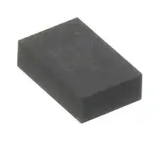
- Depth: 6.5mm
- Width: 10mm
- Height: 2.92mm
- Topology: Synchronous Buck (Step Down)
- No. of Pins: 28Pins
- Product Range: MAXM17575 Series
- No. of Outputs: 1 Output
- Output Current: 1.5A
- Output Power Max: -
- Input Voltage Max: 60V
- Input Voltage Min: 4.5V
- Output Current Max: 1.5A
- Output Voltage Max: 12V
- Output Voltage Min: 900mV
- Switching Frequency: 2.2MHz
- Input Voltage DC Max: 60V
- Input Voltage DC Min: 4.5V
- DC / DC Converter Type: SIP-28, Module
- DC / DC Converter IC Case: SIP
- Operating Temperature Max: 125°C
- Power Supply Applications: Industrial
- DC / DC Converter Output Type: Adjustable
| Delivery and price | |
|---|---|
| Units per pack | 1040 |
| Price | 6.85 € |
| Current stock | 10+ |
| Lead time | 30 days |
**EVALUATION KIT AVAILABLE**

## **MAXM17575**

## **4.5V to 60V, 1.5A High-Efficiency, DC-DC Step-Down Power Module with Integrated Inductor**

## **General Description**

The _Himalaya_ series of voltage regulator ICs and power modules enable cooler, smaller, and simpler power supply solutions. The MAXM17575 is an easy-to-use power module that combines a synchronous step-down DC-DC converter, a fully shielded inductor, and compensation components into a low-profile, thermally-efficient, systemin-package (SiP). The device operates over a wide inputvoltage range of 4.5V to 60V, delivers up to 1.5A continuous output current and has excellent line and load regulation over an output-voltage range of 0.9V to 12V.  The high level of integration significantly reduces design complexity, manufacturing risks, and offers a true plug-and-play powersupply solution, reducing time-to-market.

The MAXM17575 offers resistor-programmable switching frequency, RESET output-voltage monitoring, adjustable input undervoltage lockout, and programmable soft-start. The device also features hiccup-mode overload protection, and thermal shutdown function.

The MAXM17575 is available in a low-profile, highly thermal-emissive, compact, 28-pin 6.5mm × 10mm × 2.92mm SiP package, which reduces power dissipation and enhances efficiency. The package is easily soldered onto a printed circuit board and is suitable for automated circuit board assembly. The device can operate over the industrial temperature range from -40°C to +125°C.

## **Benefits and Features**

- Reduces Design Complexity, Manufacturing Risks, and Time-to-Market

   - Integrated Step-Down DC-DC Converter

   - Integrated Inductor

   - Integrated Compensation Components

- Saves Board Space in Space-Constrained Applications

   - Complete Integrated Step-Down Power Supply in a Single Package

   - Small Profile 6.5mm × 10mm × 2.92mm SiP Package • Simplified PCB Design with Minimal External BOM Components

- Offers Flexibility for Power-Design Optimization

   - Wide Input-Voltage Range from 4.5V to 60V

   - Output-Voltage Adjustable Range from 0.9V to 12V

   - Adjustable Frequency with External Frequency Synchronization (400kHz to 2.2MHz)

   - Soft-Start Programmable

   - PWM Mode of Operation

   - Optional Programmable EN/UVLO

- Operates Reliably in Adverse Industrial Environments

   - Integrated Thermal Fault Protection

   - Hiccup Mode Overload Protection

   - RESET Output-Voltage Monitoring

   - High Industrial Ambient Operating Temperature Range (-40°C to +125°C) / Junction Temperature Range (-40°C to +150°C)

## **Applications**

- Industrial Power Supplies

- Distributed Supply Regulation

- FPGA and DSP Point-of-Load Regulator

- Base Station Point-of-Load Regulator

- HVAC and Building Control

_**Ordering Information** appears at end of data sheet._

## **Typical Application Circuit**

**==> picture [242 x 179] intentionally omitted <==**

**----- Start of picture text -----**<br>
VIN 3.3V,1.5A<br>C1 C2<br>4.7µF VIN OUT R1 22µF<br>EN/UVLO 60.4kΩ<br>FB<br>RESET R2<br>22.6kΩ<br>RT/SYNC<br>R3 MAXM17575<br>33.2kΩ<br>SS EXTVCC_R<br>EXTVCC_C<br>SS_C<br>SGND PGND<br>LX BST VCC<br>**----- End of picture text -----**<br>


**==> picture [125 x 31] intentionally omitted <==**

_19-100080; Rev 1; 9/17_

## MAXM17575

## 4.5V to 60V, 1.5A High-Efficiency, DC-DC Step-Down Power Module with Integrated Inductor

## **Absolute Maximum Ratings**

VIN to PGND  ........................................................-0.3V to +65V EN/UVLO to SGND ....................................-0.3V to (VIN + 0.3V) EXTVCC_C to SGND ............................................-0.3V to +26V BST to PGND ........................................................-0.3V to +70V BST to LX .............................................................-0.3V to +6.0V BST to VCC ...........................................................-0.3V to +65V LX, EXTVCC_R, OUT to PGND (VIN < 25 V) ................................ -0.3V to (VIN + 0.3V) LX, EXTVCC_R, OUT to PGND (VIN > 25V) ........-0.3V to +25V

FB to SGND ...........................................................-0.3V to 1.5V RT/SYNC, SS, RESET , VCC, SS_C to SGND ......-0.3V to +6.5V PGND to SGND ....................................................-0.3V to +0.3V Output Short-Circuit Duration ....................................Continuous Operating Temperature Range (Note 1) ........... -40°C to +125°C Junction Temperature ......................................................+150°C Storage Temperature Range ............................ -40°C to +150°C Soldering Temperature (reflow) .......................................+260°C Lead Temperature (soldering, 10s) .................................+300°C

_Stresses beyond those listed under “Absolute Maximum Ratings” may cause permanent damage to the device. These are stress ratings only, and functional operation of the device at these or any other conditions beyond those indicated in the operational sections of the specifications is not implied. Exposure to absolute maximum rating conditions for extended periods may affect device reliability._

## **Package Information**

|**Package Information**|**Package Information**|
|---|---|
|**PACKAGE TYPE: 28-PIN SiP**||
|Package Code|L286510#7|
|Outline Number|**21-100180**|
|Land Pattern Number|**90-100058**|
|**THERMAL RESISTANCE, FOUR-LAYER BOARD (Note 2)**||
|Junction to Ambient (θJA)|25.5°C/W|


For the latest package outline information and land patterns (footprints), go to **www.maximintegrated.com/packages** . Note that a “+”, “#”, or “-” in the package code indicates RoHS status only. Package drawings may show a different suffix character, but the drawing pertains to the package regardless of RoHS status.

**Note 1:** Junction temperature greater than +125°C degrades operating lifetimes. **Note 2:** Package thermal resistance is measured on an evaluation board with natural convection.

Maxim Integrated │ 2

www.maximintegrated.com

## MAXM17575

## 4.5V to 60V, 1.5A High-Efficiency, DC-DC Step-Down Power Module with Integrated Inductor

## **Electrical Characteristics**

(VIN = VEN/UVLO = 24V, RRT/SYNC = 40.2kΩ, VPGND = VSGND = EXTVCC_C = 0, SS_C = SS = RESET = VCC = LX = BST = EXTVCC_R = OUT = OPEN, VFB = 1V, TA = -40°C to +125°C, unless otherwise noted. Typical values are at TA = +25°C. All voltages are referenced to SGND, unless otherwise noted) (Note 3)

|**PARAMETER**|**SYMBOL**|**CONDITIONS**|**MIN**<br>**TYP**<br>**MAX**|**UNITS**|
|---|---|---|---|---|
|**INPUT SUPPLY (VIN )**|||||
|Input-Voltage Range|VIN||4.5<br>60|V|
|Input-Shutdown Current|IIN(SH)|VEN/UVLO= 0V (shutdown mode)|12<br>16|μA|
|Input-Quiescent Current|IQ_PWM|Normal switching mode,<br>VOUT= 5.0V, fSW= 900kHz,<br>EXTVCC_C = EXTVCC_R|7.7|mA|
|**EN/UVLO (EN)**|||||
|EN/UVLO Threshold|VENR|VEN/UVLOrising|1.19<br>1.215<br>1.26|V|
||VENF|VEN/UVLOfalling|1.068<br>1.09<br>1.131||
|EN/UVLO Pullup Resistor|RENP|Pullup resistor between VINand EN/<br>UVLO pins|3.15<br>3.3<br>3.45|MΩ|
|**LDO (VCC)**|||||
|VCCOutput-Voltage Range|VCC|1mA ≤ IVCC≤ 15mA|4.75<br>5<br>5.25|V|
|||6V ≤ VIN≤ 60V; IVCC= 1mA|4.75<br>5<br>5.25||
|VCCCurrent Limit|IVCC(MAX)|VCC= 4.3V, VIN= 6.5V|25<br>54<br>100|mA|
|VCCDropout|VCC(DO)|VIN= 4.5V , IVCC= 15mA|0.35|V|
|VCCUVLO|VCC(UVR)|Vcc rising|4.05<br>4.2<br>4.3|V|
||VCC(UVF)|Vcc falling|3.65<br>3.8<br>3.9||
|**EXT LDO (EXTVCC_C)**|||||
|EXTVCC_C Switch-Over<br>Voltage||EXTVCC_C rising|4.56<br>4.7<br>4.84|V|
|||EXTVCC_C falling|4.3<br>4.45<br>4.6||
|EXTVCC_C Dropout|EXTVCC(DO)|EXTVCC_C = 4.75V , IEXTVCC= 15mA|0.3|V|
|EXTVCC_C Current Limit|EXT VCC_CILIM|VCC= 4.5V, EXTVCC_C = 7V|26.5<br>60<br>100|mA|
|**SOFT-START (SS)**|||||
|Soft-Start Current|ISS|VSS= 0.5V|4.7<br>5<br>5.3|μA|
|**OUTPUT SPECIFICATIONS**|||||
|Line-Regulation Accuracy||VOUT= 5V|0.1|mV/V|
|Load-Regulation Accuracy|||1|mV/A|
|FB Regulation Voltage|VFB_REG||0.889<br>0.9<br>0.911|V|
|FB Input-Bias Current|IFB|0V ≤ VFB≤ 1V, TA= 25°C|-50<br>+50|nA|
|FB Undervoltage Trip Level<br>to Cause HICCUP|VFB(HICF)||0.56<br>0.58<br>0.65|V|
|HICCUP Timeout|||32768|Cycles|
|**CURRENT LIMIT**|||||
|Average Current-Limit<br>Threshold|IAVG(LIMIT)|VOUT= 5V, fSW= 900kHz|1.86|A|


Maxim Integrated │ 3

www.maximintegrated.com

## MAXM17575

## 4.5V to 60V, 1.5A High-Efficiency, DC-DC Step-Down Power Module with Integrated Inductor

## **Electrical Characteristics (continued)**

(VIN = VEN/UVLO = 24V, RRT/SYNC = 40.2kΩ, VPGND = VSGND = EXTVCC_C = 0, SS_C = SS = RESET = VCC = LX = BST = EXTVCC_R = OUT = OPEN, VFB = 1V, TA = -40°C to +125°C, unless otherwise noted. Typical values are at TA = +25°C. All voltages are referenced to SGND, unless otherwise noted) (Note 3)

|**PARAMETER**|**SYMBOL**|**CONDITIONS**|**MIN**<br>**TYP**<br>**MAX**|**UNITS**|
|---|---|---|---|---|
|**RRT/SYNC**|||||
|Switching Frequency|fSW|RRT= OPEN|430<br>490<br>550|kHz|
|||RRT= 51.1KΩ|370<br>400<br>430||
|||RRT= 40.2KΩ|475<br>500<br>525||
|||RRT= 8.06KΩ|1950<br>2200<br>2450||
|Synchronization Frequency-<br>Capture Range||fSWset by RRT|1.1 × fSW<br>1.4 × fSW||
|Synchronization Pulse Width|||50|ns|
|Synchronization Threshold|VIL||0.8|V|
||VIH||2.1||
|Minimum On-Time|tON_MIN||60<br>80|ns|
|Minimum Off-Time|tOFF_MIN||140<br>150<br>160|ns|
|**RESET**|||||
|RESETOutput-Level Low||IRESET= 10mA|400|mV|
|RESETOutput-Leakage<br>Current||TA= TJ= 25°C, VRESET= 5.5V|-100<br>100|nA|
|VOUTThreshold forRESET<br>Assertion|VOUT(OKF)|VFBfalling|90.5<br>92<br>94.6|%|
|VOUTThreshold forRESET<br>Deassertion|VOUT(OKR)|VFBrising|93.8<br>95<br>97.8|%|
|RESETDelay after FB<br>Reaches 95% Regulation|||1024|Cycles|
|**THERMAL SHUTDOWN**|||||
|Thermal Shutdown<br>Threshold|TSHDNR|Temp rising|165|ºC|
|Thermal Shutdown<br>Hysteresis|TSHDNHY||10|ºC|


**Note 3:** Electrical specification are production tested at TA = +25°C. Specifications over the entire operating range is guaranteed by design and characterization.

Maxim Integrated │ 4

www.maximintegrated.com

## MAXM17575

## 4.5V to 60V, 1.5A High-Efficiency, DC-DC Step-Down Power Module with Integrated Inductor

## **Typical Operating Characteristics**

(VIN = 24V, VSGND = VPGND = 0V, TA = -40°C to +125°C, unless otherwise noted. Typical values are at TA = +25°C. All voltages are referenced to SGND, unless otherwise noted. The circuit values for different output voltage applications are as in Table 1, unless otherwise noted.)

**==> picture [691 x 557] intentionally omitted <==**

**----- Start of picture text -----**<br>
EFFICIENCY vs. LOAD CURRENT EFFICIENCY vs. LOAD CURRENT EFFICIENCY vs. LOAD CURRENT<br>(VOUT = 0.9V, fSW = 400kHz) (VOUT = 1.2V, fSW = 400kHz) (VOUT = 1.8V, fSW = 400kHz)<br>100 toc01 100 toc02 100 toc03<br>90 90 90<br>80 80 80<br>70 70 70 VIN = 4.5V<br>60 VIN = 4.5V VIN = 4.5V 60<br>60 VIN = 12V<br>50 VIN = 12V 50 VIN = 12V 50 VIN = 24V<br>40 40<br>40<br>30 VIN = 24V 30 VIN = 36V<br>30<br>20 20<br>20<br>10 10<br>10<br>0 0<br>0 300 600 900 1200 1500 0 0 300 600 900 1200 1500<br>0 300 600 900 1200 1500<br>LOAD CURRENT (mA) LOAD CURRENT (mA)<br>LOAD CURRENT (mA)<br>EFFICIENCY vs. LOAD CURRENT EFFICIENCY vs LOAD CURRENT EFFICIENCY vs. LOAD CURRENT<br>100 (VOUT = 2.5V, fSW = 490kHz) toc04 100 (VOUT = 3.3V, fSW = 600kHz) toc05 100 (VOUT = 5V, fSW = 900kHz) toc06<br>90 90 90<br>80 80 80<br>70 VIN = 4.5V 70 70<br>60 VIN = 12V 60 VIN = 12V 60 VIN = 12V<br>50 VIN = 24V 50 50 VIN = 24V<br>40 40 VIN = 24V 40<br>30 VIN = 48V 30 VIN = 48V 30 VIN = 48V<br>20 VIN = 60V 20 VIN = 60V 20 VIN = 60V<br>10 10 10<br>0 0 300 600 900 1200 1500 0 0 300 600 900 1200 1500 0 0 300 600 900 1200 1500<br>LOAD CURRENT (mA) LOAD CURRENT (mA) LOAD CURRENT (mA)<br>EFFICIENCY vs. LOAD CURRENT EFFICIENCY vs. LOAD CURRENT OUTPUT VOLTAGE (3.3V)<br>(VOUT = 8V, fSW = 1500kHz) (VOUT = 12V, fSW = 2200kHz) vs. LOAD CURRENT<br>100 toc07 100 toc08 3.31 toc09<br>90 90 3.309<br>80 80 3.308<br>70 VIN = 12V 70 VIN = 21V 3.307 VIN = 12V<br>60 60 VIN = 24V 3.306 VIN = 48V<br>50 VIN = 24V 50 3.305<br>40 VIN = 48V 40 VIN = 48V 3.304<br>30 30 3.303<br>20 VIN = 60V 20 VIN = 60V 3.302 VIN = 24V<br>10 10 3.301 VIN = 60V<br>0<br>3.3<br>0 300 600 900 1200 1500 0<br>0 300 600 900 1200 1500 0 300 600 900 1200 1500<br>LOAD CURRENT (mA) LOAD CURRENT (mA) LOAD CURRENT (mA)<br>(%) (%) (%)<br>EFFICIENCY EFFICIENCY<br>EFFICIENCY<br>(%) (%) (%)<br>EFFICIENCY EFFICIENCY EFFICIENCY<br>(%) (%)<br>EFFICIENCY<br>EFFICIENCY<br>OUTPUT  VOLTAGE (V)<br>**----- End of picture text -----**<br>


Maxim Integrated │ 5

www.maximintegrated.com

## MAXM17575

## 4.5V to 60V, 1.5A High-Efficiency, DC-DC Step-Down Power Module with Integrated Inductor

## **Typical Operating Characteristics (continued)**

(VIN = 24V, VSGND = VPGND = 0V, TA = -40°C to +125°C, unless otherwise noted. Typical values are at TA = +25°C. All voltages are referenced to SGND, unless otherwise noted. The circuit values for different output voltage applications are as in Table 1, unless otherwise noted.)

**==> picture [493 x 521] intentionally omitted <==**

**----- Start of picture text -----**<br>
OUTPUT VOLTAGE (5V) OUTPUT VOLTAGE (3.3V)  OUTPUT VOLTAGE (5.0V)<br>vs. LOAD CURRENT vs. INPUT VOLTAGE vs. INPUT VOLTAGE<br>5.155.14 || toc10 3.3103.309 toc11 5.110 toc12<br>5.13 3.308<br>5.12 F VIN = 24V VIN = 12V s 3.307 5.100 =<br>5.11 3.306 IOUT = 0.5A<br>5.1 a aa 3.305 5.090 IOUT = 1A IOUT = 1.5A<br>5.095.08 P A VIN = 48V P VIN = 60V 3.304 OgeeeeeeeeCsd[']sd 5.080<br>3.303<br>5.07 a oe 3.302 = IOUT —  = 0A IOUT —  = 0.5A —— 5.070 ae IOUT = 0A<br>5.06 3.301 IOUT = 1A IOUT = 1.5A<br>5.05 0 a 300 600 900 1200 1500 3.300 oo fo 5.060 0 T 10 20 30 I 40 50 60<br>0 10 20 30 40 50 60<br>LOAD CURRENT (mA) INPUT VOLTAGE (V)<br>INPUT VOLTAGE (V)<br>OUTPUT-VOLTAGE RIPPLE OUTPUT-VOLTAGE RIPPLE<br>(VIN = 24V, VOUT = 3.3V, IOUT = 1.5A) toc13 (VIN = 24V, VOUT = 5V, IOUT = 1.5A) toc14<br>VOUT (AC) 10mV/div VOUT (AC) 10mV/div<br>1µs/div 1µs/div<br>LOAD TRANSIENT RESPONSE LOAD TRANSIENT RESPONSE<br>(VIN = 24V, VOUT = 3.3V, IOUT = 0A TO 0.75A) (VIN = 24V, VOUT = 3.3V, IOUT = 0.75A TO 1.5A)<br>toc15 toc16<br>100mV/div<br>VOUT (AC) 100mV/div VOUT (AC)<br>500mA/div<br>IOUT 500mA/div IOUT<br>20µs/div 20µs/div<br>OUTPUT  VOLTAGE (V)<br>OUTPUT  VOLTAGE (V)<br>OUTPUT  VOLTAGE (V)<br>**----- End of picture text -----**<br>


Maxim Integrated │ 6

www.maximintegrated.com

## MAXM17575

## 4.5V to 60V, 1.5A High-Efficiency, DC-DC

## Step-Down Power Module with Integrated Inductor

## **Typical Operating Characteristics (continued)**

(VIN = 24V, VSGND = VPGND = 0V, TA = -40°C to +125°C, unless otherwise noted. Typical values are at TA = +25°C. All voltages are referenced to SGND, unless otherwise noted. The circuit values for different output voltage applications are as in Table 1, unless otherwise noted.)

**==> picture [435 x 512] intentionally omitted <==**

**----- Start of picture text -----**<br>
LOAD TRANSIENT RESPONSE LOAD TRANSIENT RESPONSE,<br>(VIN = 24V, VOUT = 5.0V, IOUT = 0A TO 0.75A) (VIN = 24V, VOUT = 5.0V, IOUT = 0.75A TO 1.5A)<br>toc17 toc18<br>VOUT (AC) 100mV/div<br>VOUT (AC) 100mV/div<br>FIGURE6<br>APPLICATION CIRCUIT<br>VOUT=5V<br>500mA/div<br>IOUT 500mA/div IOUT<br>=<br>20µs/div<br>20µs/div<br>STEADY-STATE LX AND OUTPUT VOLTAGE STEADY-STATE LX AND OUTPUT VOLTAGE<br>(VIN = 24V, VOUT = 3.3V, IOUT = 1.5A) (VIN = 24V, VOUT = 5.0V, IOUT = 1.5A)<br>toc19 toc20<br>1V/div<br>2V/div<br>VOUT VOUT<br>10V/div<br>10V/div<br>LX LX ITT<br>1µs/div 1µs/div<br>STARTUP THROUGH ENABLE SHUTDOWN THROUGH ENABLE<br>(VIN = 24V, VOUT = 3.3V, LOAD RESISTANCE = 2.2Ω) (VIN = 24V, VOUT = 3.3V, LOAD RESISTANCE = 2.2Ω)<br>toc21 toc22<br>5V/div VEN/UVLO<br>VEN/UVLO 20V/div<br>5V/div<br>LX LX<br>2V/div VOUT 20V/div<br>VOUT 5V/div<br>RESET 2V/div<br>RESET 5V/div<br>a e f e<br>1ms/div<br>100µs/div<br>**----- End of picture text -----**<br>


Maxim Integrated │ 7

www.maximintegrated.com

## MAXM17575

## 4.5V to 60V, 1.5A High-Efficiency, DC-DC

## Step-Down Power Module with Integrated Inductor

##

##

(VIN = 24V, VSGND = VPGND = 0V, TA = -40°C to +125°C, unless otherwise noted. Typical values are at TA = +25°C. All voltages are referenced to SGND, unless otherwise noted. The circuit values for different output voltage applications are as in Table 1, unless otherwise noted.)

## **STARTUP THROUGH ENABLE**

## **SHUTDOWN THROUGH ENABLE**

**==> picture [164 x 143] intentionally omitted <==**

**----- Start of picture text -----**<br>
(VIN = 24V, VOUT = 5V, LOAD RESISTANCE = 3.3Ω)IN = 24V, VOUT = 5V, LOAD RESISTANCE = 3.3Ω) = 24V, VOUT = 5V, LOAD RESISTANCE = 3.3Ω)OUT = 5V, LOAD RESISTANCE = 3.3Ω) = 5V, LOAD RESISTANCE = 3.3Ω)<br>toc23<br>5V/div<br>VEN/UVLOEN/UVLO 20V/div<br>LX<br>2V/div<br>2V/div<br>VOUTOUT<br>RESET<br>1ms/div<br>**----- End of picture text -----**<br>


**==> picture [420 x 500] intentionally omitted <==**

**----- Start of picture text -----**<br>
(VIN = 24V, VOUT = 5V, LOAD RESISTANCE = 3.3Ω)IN = 24V, VOUT = 5V, LOAD RESISTANCE = 3.3Ω) = 24V, VOUT = 5V, LOAD RESISTANCE = 3.3Ω)OUT = 5V, LOAD RESISTANCE = 3.3Ω) = 5V, LOAD RESISTANCE = 3.3Ω) (VIN = 24V, VOUT = 5V, LOAD RESISTANCE = 3.3Ω)<br>toc23 toc24<br>5V/div VEN/UVLO<br>VEN/UVLOEN/UVLO 20V/div 5V/div<br>LX LX<br>2V/div<br>20V/div<br>2V/div<br>VOUT<br>VOUTOUT 5V/div<br>RESET<br>RESET 5V/div<br>1ms/div 100µs/div<br>STARTUP WITH 2.5V PREBIAS STARTUP THROUGH INPUT SUPPLY<br>(LOAD CURRENT 10mA) (VIN = 24V, VOUT = 3.3V, LOAD CURRENT 1.5A)<br>toc25 toc26<br>10V/div<br>5V/div<br>VEN/UVLO 20V/div<br>LX VIN<br>2V/div<br>2V/div<br>1A/div<br>VOUT<br>VOUT 5V/div IOUT 5V/div<br>RESET RESET<br>a<br>1ms/div 1ms/div<br>STARTUP THROUGH INPUT SUPPLY OUTPUT SHORT DURING STARTUP<br>(VIN = 24V, VOUT = 5V, LOAD CURRENT 1.5A) (VIN = 24V, VOUT = 3.3V, IOUT = 1.5A)<br>toc27 toc28<br>10V/div 10V/div<br>2V/div<br>VIN VIN<br>50mV/div<br>VOUT<br>1A/div<br>VOUT 20V/div<br>IOUT 5V/div LX<br>RESET IOUT 5A/div<br>1ms/div 20ms/div<br>**----- End of picture text -----**<br>


Maxim Integrated │ 8

www.maximintegrated.com

## MAXM17575

## 4.5V to 60V, 1.5A High-Efficiency, DC-DC

## Step-Down Power Module with Integrated Inductor

## **Typical Operating Characteristics (continued)**

(VIN = 24V, VSGND = VPGND = 0V, TA = -40°C to +125°C, unless otherwise noted. Typical values are at TA = +25°C. All voltages are referenced to SGND, unless otherwise noted. The circuit values for different output voltage applications are as in Table 1, unless otherwise noted.)

**==> picture [418 x 518] intentionally omitted <==**

**----- Start of picture text -----**<br>
OUTPUT SHORT IN STEADY STATE OUTPUT SHORT DURING STARTUP<br>(VIN = 24V, VOUT = 3.3V, IOUT = 1.5A) (VIN = 24V, VOUT = 5V, IOUT = 1.5A)<br>toc29 toc30<br>10V/div 10V/div<br>VIN 50mV/div VIN<br>50mV/div<br>VOUT — VOUT ropetentotentete<br>20V/div 20V/div<br>LX<br>LX<br>IOUT 5A/div IOUT 5A/div<br>20ms/div 20ms/div<br>OUTPUT SHORT IN STEADY STATE EXTERNAL SYNCHRONIZATION<br>(VIN = 24V, VOUT = 5.0V, IOUT = 1.5A) (VIN = 24V, VOUT = 3.3V, IOUT = 1.5A)<br>toc31 toc32<br>10V/div<br>5V/div<br>SYNC<br>“NNN<br>10V/div<br>VIN<br>VOUT 50mV/div<br>20V/div LX<br>2V/div<br>LX<br>IOUT 5A/div VOUT<br>20ms/div 4µs/div<br>EXTERNAL SYNCHRONIZATION EXTVCC SWITCHOVER VOLTAGE<br>(VIN = 24V, VOUT = 5V, IOUT = 1.5A) (VIN = 24V, VOUT = 5V, IOUT = 1.5A)<br>toc33 toc34<br>5V/div 1V/div<br>SYNC MN 1V/div<br>10V/div<br>LX<br>5V/div<br>VCC<br>VOUT VOUT<br>2µs/div<br>400µs/div<br>**----- End of picture text -----**<br>


Maxim Integrated │ 9

www.maximintegrated.com

## MAXM17575

## 4.5V to 60V, 1.5A High-Efficiency, DC-DC

## Step-Down Power Module with Integrated Inductor

## **Typical Operating Characteristics (continued)**

(VIN = 24V, VSGND = VPGND = 0V, TA = -40°C to +125°C, unless otherwise noted. Typical values are at TA = +25°C. All voltages are referenced to SGND, unless otherwise noted. The circuit values for different output voltage applications are as in Table 1, unless otherwise noted.)

**==> picture [531 x 367] intentionally omitted <==**

**----- Start of picture text -----**<br>
0.9V OUTPUT BODE  1.2V OUTPUT BODE  1.8V OUTPUT BODE<br>(VIN = 12V, LOAD CURRENT 1.5A) (VIN = 24V, LOAD CURRENT 1.5A) (VIN = 24V, LOAD CURRENT 1.5A)<br>toc35 toc36 toc37<br>60 150 40 100 40 150<br>30<br>40 100 100<br>20<br>50 20<br>20 50 50<br>10<br>0 0<br>0 0 0 0<br>-20 -50 -20 -50 -10 -50<br>CROSSOVER  CROSSOVER  CROSSOVER<br>FREQUENCY = 52.19kHz FREQUENCY = 45.23kHz -20 FREQUENCY = 45.45kHz<br>-40 1K PHASE MARGIN = 60.44610k ᵒ 100k -100 -401K PHASE MARGIN = 60.11310k ᵒ 100k -100 -301K PHASE MARGIN = 62.12810k ᵒ 100k -100<br>FREQUENCY (Hz)<br>FREQUENCY (Hz) FREQUENCY (Hz)<br>2.5V OUTPUT BODE  3.3V OUTPUT BODE<br>(VIN = 24V, LOAD CURRENT 1.5A) (VIN = 24V, LOAD CURRENT 1.5A)<br>toc38 toc39<br>40 40<br>30 100 30 100<br>a ms ,<br>20 20<br>50 50<br>10 10<br>0 0 0 0<br>S| &<br>-10 -10<br>-50 -50<br>-20 CROSSOVER  -20 CROSSOVER<br>FREQUENCY = 47.58kHz FREQUENCY = 53.37kHz<br>PHASE MARGIN = 61.447 ᵒ PHASE MARGIN = 65.490 ᵒ<br>-30 -100 -30 -100<br>1K 10k 100k 1K 10k 100k<br>FREQUENCY (Hz)<br>FREQUENCY (Hz)<br>GAIN (dB) GAIN (dB)<br>GAIN (dB)    PHASE MARGIN (°)<br>PHASE MARGIN (°)<br>PHASE MARGIN (°)<br>GAIN (dB) GAIN (dB)<br>PHASE MARGIN (°)<br>PHASE MARGIN (°)<br>**----- End of picture text -----**<br>


Maxim Integrated │ 10

www.maximintegrated.com

## MAXM17575

## 4.5V to 60V, 1.5A High-Efficiency, DC-DC

## Step-Down Power Module with Integrated Inductor

##

##

(VIN = 24V, VSGND = VPGND = 0V, TA = -40°C to +125°C, unless otherwise noted. Typical values are at TA = +25°C. All voltages are referenced to SGND, unless otherwise noted. The circuit values for different output voltage applications are as in Table 1, unless otherwise noted.)

**==> picture [424 x 360] intentionally omitted <==**

**----- Start of picture text -----**<br>
5.0V OUTPUT BODE  8.0V OUTPUT BODE<br>(VIN = 24V, LOAD CURRENT 1.5A) (VIN = 24V, LOAD CURRENT 1.5A)<br>toc40 toc41<br>100 40 100<br>40 30<br>20 50<br>50<br>20<br>10<br>0 0<br>0 = 0<br>-10<br>CROSSOVER  -20 CROSSOVER  -50<br>-20 FREQUENCY = 45.18kHzPHASE MARGIN = 70.333 ᵒ -50 FREQUENCY = 49.29kHzPHASE MARGIN = 70.265 ᵒ<br>-30 ness<br>1K is 10k 100k 1K 10k | 100k A<br>FREQUENCY (Hz) FREQUENCY (Hz)<br>12V OUTPUT BODE  AMBIENT TEMPERATURE vs. OUTPUT CURRENT<br>(VIN = 24V, LOAD CURRENT 1.5A) (VIN = 24V, NO AIR FLOW)<br>toc42 toc43<br>40 100<br>1.5<br>30<br>1.3<br>20 50 VOUT = 3.3V<br>Simm C OC A<br>10 1.1 VOUT = 5.0V<br>0 PSN)o™ 0 0.9 Ha a VOUT = 12.0V AV"e<br>-10<br>0.7 Poor<br>CROSSOVER<br>-20 -50<br>FREQUENCY = 46.86kHz<br>-30 PHASE MARGIN = 71.356 ᵒ ceo SN 0.5 Pe| | EN<br>0.0 20.0 40.0 60.0 80.0 100.0 120.0 140.0<br>1K 10k 100k<br>FREQUENCY (Hz) AMBIENT TEMPERATURE (ᵒC)<br>GAIN (dB)<br>GAIN (dB)<br>PHASE MARGIN (°) PHASE MARGIN (°)<br>(A)<br>GAIN (dB)<br>PHASE MARGIN (°) OUTPUT CURRENT<br>**----- End of picture text -----**<br>


Maxim Integrated │ 11

www.maximintegrated.com

## MAXM17575

## 4.5V to 60V, 1.5A High-Efficiency, DC-DC Step-Down Power Module with Integrated Inductor

## **Pin Configuration**

|TOP VIEW|||VIN|VIN||VIN||VIN|||PGND||PGND|PGND|PGND|PGND|OUT|OUT||OUT||OUT||OUT||||
|---|---|---|---|---|---|---|---|---|---|---|---|---|---|---|---|---|---|---|---|---|---|---|---|---|---|---|---|
||+|||||||||||||||||||||||||||
|||||1||28||27|||26||25||24|||23||22||21||20||||
|||||||||||||||||||||||||||||
|EN/UVLO||||2||||||||||||||||||||19|||OUT|
|||||||||||||||||||||||||||||
|RESET||||3||||||||||||||||||||18|||OUT|
|||||||||EP1|||||||EP3||||||EP2|||||||
|SS||||4||||||||||||||||||||17|||OUT|
|||||||||||||||||||||||||||||
|VCC||||5||||||||||||||||||||16|||OUT|
|||||||||||||||||||||||||||||
|||||6||7||8|||9||10||11|||12||13||14||15||||
|||||||||||||||||||||||||||||
|||||NC||SS_C|RT/SYNC|||SGND|||FB||SGND||BST|||LX|EXTVCC_C<br>EXTVCC_R|||||||
|||||||||||||6.5mm × 10mm ×|||2.92mm|||||||||||||


Maxim Integrated │ 12

www.maximintegrated.com

## MAXM17575

## 4.5V to 60V, 1.5A High-Efficiency, DC-DC Step-Down Power Module with Integrated Inductor

## **Pin Description**

|**PIN**|**NAME**|**FUNCTION**|
|---|---|---|
|1, 27, 28|VIN|Power-Supply Input. Connect the VINpins together. Decouple to PGND with a capacitor; place the<br>capacitor close to the VINand PGND pins.|
|2|EN/UVLO|Enable/Undervoltage Lockout Input. Connect a resistor from EN/UVLO to SGND to set the UVLO<br>threshold. See the_Input Undervoltage-Lockout Levelt_section for more details.|
|3|RESET|Open-DrainRESETOutput. TheRESEToutput is driven low if FB drops below 92% of its set value.<br>RESETgoes high 1024 clock cycles after FB rises above 95% of its set value.|
|4|SS|Soft-Start Input. Connect a capacitor from SS to SGND to set the soft-start time.|
|5|VCC|5V LDO Output. The VCCis bypassed to PGND internally through a 2.2µF capacitor. Do not connect<br>external components to the VCCpin.|
|6|NC|Not Connected|
|7|SS_C|Soft-Start Capacitor Node. Internally a 5600pF is connected from SS_C to SGND. Connect this pin<br>with a  short trace to SS to use the internal cap for the soft-start function.|
|8|RT/SYNC|Oscillator Timing Resistor Input. Connect a resistor from RT/SYNC to SGND to program the switching<br>frequency from 400kHz to 2.2MHz. An external pulse can be applied to RT/SYNC  through a coupling<br>capacitor to synchronize the internal clock to the external pulse frequency.|
|9, 11|SGND|Analog Ground.|
|10|FB|Feedback Input. Connect FB node to the junction of the external feedback divider network from the<br>OUT to SGND to set the output voltage.|
|12|BST|Boost Flying Capacitor Node. Internally a 0.1μF is connected from BST to LX. Do not connect<br>external components to BST pin.|
|13|LX|Internally Shorted to Switching Node. Do not connect external components to LX pin.|
|14|EXTVCC_C|External Power-Supply Input for the Internal LDO. For applications with output voltage > 5V, connect<br>EXTVCC_C to EXTVCC_R pin to improve the effciency. For other applications, EXTVCC_C should<br>be connected to SGND.|
|15|EXTVCC_R|Input Pin for the EXTVCC_C Supply. Connect to EXTVCC_C for an output voltage ≥ 5V. When this<br>function is unused, EXTVCC_R should be left OPEN. Other than EXTVCC_C, do not connect any<br>external components to EXTVCC_R.|
|16–23|OUT|Regulator Output Pin. Connect a capacitor from OUT to PGND. See the_PCB Layout Guidelines_sec-<br>tion for connection details.|
|24–26|PGND|Power Ground. Connect the PGND pins externally to the power ground plane.|
|EP1|SGND|Exposed Pad. Connect to the SGND of the module. Connect to a large copper plane below the IC to<br>improve heat dissipation capability.|
|EP2|OUT|Exposed Pad. Connect to the OUT pins of the module. Connect to a large copper plane below the IC<br>to improve heat dissipation capability.|
|EP3|NC|Exposed Pad. Not connected|


Maxim Integrated │ 13

www.maximintegrated.com

## MAXM17575

## 4.5V to 60V, 1.5A High-Efficiency, DC-DC Step-Down Power Module with Integrated Inductor

## **Functional Diagram**

**==> picture [505 x 571] intentionally omitted <==**

**----- Start of picture text -----**<br>
MAXM17575<br>VCC VIN<br>LDO<br>0.1µF<br>2.2µF<br>SGND BST<br>0.1µF<br>VIN<br>3.3MΩ<br>EN/UVLO LX<br>1.215V<br>PEAK  4.7µH<br>RT/SYNC OSCILLATOR CURRENT-MODE  OUT<br>CONTROLLER<br>1µF<br>FB PGND<br>OUT<br>4.7Ω<br>EXTVCC_R<br>SS<br>EXTVCC_C<br>0.1µF<br>SS_C<br>5600pF<br>RESET<br>FB<br>RESET<br>LOGIC<br>**----- End of picture text -----**<br>


Maxim Integrated │ 14

www.maximintegrated.com

## MAXM17575

## 4.5V to 60V, 1.5A High-Efficiency, DC-DC Step-Down Power Module with Integrated Inductor

## **Detailed Description**

The MAXM17575 is a high-efficiency, high-voltage stepdown power module with dual-integrated MOSFETs that operates over a 4.5V to 60V input and supports a programmable output voltage from 0.9V to 12V, delivering up to 1.5A current. The MAXM17575 module integrates all the necessary components required for switching the converter. Built-in compensation for the entire output-voltage range eliminates the need for external components.

The MAXM17575 features a peak-current-mode control architecture and operates the device in pulse-width modulation (PWM) mode providing a constant frequency operation at all loads, and is useful in applications sensitive to variable switching frequency. The device also features an RT/SYNC pin to program the switching frequency. A programmable soft-start feature allows users to reduce input inrush current. The device also incorporates an output enable/undervoltage lockout pin (EN/UVLO) that allows the user to turn on the part at the desired input-voltage level. An open-drain RESET pin provides a delayed power-good signal to the system upon achieving successful regulation of the output voltage.

## **Linear Regulator**

The MAXM17575 has two internal low dropout (LDO) regulators that powers VCC. One LDO is powered from VIN (LDO) and the other LDO is powered from EXTVCC_C (EXTLDO). During power-up, when the Enable pin voltage is above the true shutdown voltage, then the VCC is powered from LDO. When VCC voltage is above the VCC UVLO threshold and EXTVCC_C voltage is greater than 4.7V (typ), then the VCC is powered from EXTLDO. Only one of the two LDOs is in operation at a time, depending on the voltage levels present at EXTVCC_C. Powering VCC from EXTLDO increases efficiency at higher input voltages. EXTVCC_C voltage should not exceed 24V.

The typical VCC output voltage is 5V. In applications where the buck converter output is connected to the EXTVCC_C pin, if the output is shorted to ground, then transfer from EXTLDO to the LDO happens seamlessly without any impact on the normal functionality.

## **External Frequency Synchronization (RT/SYNC)**

The internal oscillator of the MAXM17575 can be synchronized to an external clock signal through the RT/ SYNC pin. The external clock should be coupled to the RT/SYNC pin using the circuit as shown in Figure 1. The external synchronization clock frequency must be between 1.1 × fSW and 1.4 × fSW, where fSW is

the frequency programmed by the RT resistor (RRT). When an external clock is applied to the RT/SYNC pin, the internal oscillator frequency changes to external clock frequency (from original frequency based on the RT setting) after detecting 16 external clock edges. The minimum external clock high pulse width and amplitude should be greater than 50ns and 2.1V respectively. The maximum external clock low pulse amplitude should be less than 0.8V.

## **Operating Input-Voltage Range**

The minimum and maximum operating input voltages for a given output voltage should be calculated as follows:

**==> picture [239 x 85] intentionally omitted <==**

where,

VOUT = Steady-state output voltage,

IOUT(MAX) = Maximum load current,

fSW(MAX) = Maximum switching frequency,

tOFF_MIN(MAX) = Worst-case minimum switch off-time (160ns) tON_MIN(MAX) = Worst-case minimum switch on-time (80ns) fSW(MIN) = Minimum switching frequency

Table 1 provides operating input voltage range and optimum switching switching frequency for different selected output voltages.

**==> picture [242 x 169] intentionally omitted <==**

**----- Start of picture text -----**<br>
MAXM17575<br>RT/SYNC<br>RRT<br>33.2kΩ  C2<br>47pF<br>C1<br>100pF<br>CLOCK<br>SOURCE R1 D1<br>1kΩ<br>VLOGIC_HIGH<br>VLOGIC_LOW<br>**----- End of picture text -----**<br>


_Figure 1. External Clock Synchronization_

Maxim Integrated │ 15

www.maximintegrated.com

## MAXM17575

## 4.5V to 60V, 1.5A High-Efficiency, DC-DC Step-Down Power Module with Integrated Inductor

## **RESET Output**

The device includes a RESET pin to monitor the output voltage. The open-drain RESET output requires an external pullup resistor. RESET goes high-impedance 1024 switching cycles after the regulator output increases above 95% of the designed nominal regulated voltage. RESET goes low when the regulator output voltage drops below 92% of the nominal regulated voltage. RESET also goes low during thermal shutdown.

## **Thermal Fault Protection**

The MAXM17575 features a thermal-fault protection circuit. When the junction temperature rises above 165°C (typ), a thermal sensor activates the fault latch, pulls down the RESET output, and shuts down the regulator. The controller soft-starts after the junction temperature cools down by 10°C.

## **Overcurrent Protection (OCP)**

The device is provided with a robust overcurrent protection (OCP) scheme that protects the device under overload and output short-circuit conditions. When the overcurrent occurs or the FB voltage falls below 0.58V (typ), the module enters into hiccup mode of operation. In hiccup mode, the converter is protected by suspending switching for a hiccup timeout period of 32,768 clock cycles. Once the hiccup timeout period expires, soft-start is attempted again. Hiccup mode of operation ensures low power dissipation under output short-circuit conditions.

## **Applications Information**

## **Input-Capacitor Selection**

The input capacitor serves to reduce the current peaks drawn from the input power supply and reduces switching noise from the module. The input capacitor values in Table 1 are the minimum recommended values for desired input and output voltages. Applying capacitor values larger than those indicated in Table 1 are acceptable to improve the dynamic response. For further operating conditions, the

total input capacitance must be greater than or equal to the value given by the following equation in order to keep the input-voltage ripple within specifications and to minimize the high-frequency ripple current being fed back to the input source:

**==> picture [98 x 26] intentionally omitted <==**

where IIN(AVG) is the average input current given by:

**==> picture [77 x 24] intentionally omitted <==**

## and where,

D = The operating duty cycle, which is approximately equal to VOUT/VIN.

∆VIN = The required input-voltage ripple.

fSW = The operating switching frequency.

POUT = The out power, which is equal to VOUT × IOUT.

## η = The efficiency.

The input capacitor must meet the ripple-current requirement imposed by the switching currents. The RMS inputripple current is given by:

**==> picture [186 x 29] intentionally omitted <==**

The worst-case RMS current requirement occurs when operating with D = 0.5. At this point, the above equation simplifies to IRMS = 0.5 x IOUT.

In applications where the source is located distant from the device input, an electrolytic capacitor should be added in parallel to the ceramic capacitor to provide necessary damping for potential oscillations caused by the inductance of the longer input power path and input ceramic capacitor. Choose an input capacitor that exhibits less than +10°C temperature rise at the RMS input current for optimal circuit longevity.

Maxim Integrated │ 16

www.maximintegrated.com

## MAXM17575

## 4.5V to 60V, 1.5A High-Efficiency, DC-DC Step-Down Power Module with Integrated Inductor

## **Output-Capacitor Selection**

The X7R ceramic output capacitors are preferred due to their stability over temperature in industrial applications. The minimum recommended output capacitor values are listed in Table 1 for desired output voltages to support a dynamic step load of 50% of the maximum output current and to contain the output-voltage deviation to 3% of the

output voltage. For additional adjustable output voltages, the output capacitance value is derived from the following equation:

**==> picture [65 x 24] intentionally omitted <==**

where COUT is the output capacitance in μF

**Table 1. Selection of Component Values**

|**VIN(MIN)**<br>**(V)**|**VIN(MAX)**<br>**(V)**|**VOUT**<br>**(V)**|**CIN**|**COUT**|**RU**<br>**(kΩ)**|**RB**<br>**(kΩ)**|**fSW**<br>**(kHz)**|**RRT**<br>**(kΩ)**|**CSS**<br>**(PF)**|
|---|---|---|---|---|---|---|---|---|---|
|4.5|15|0.9|1 × 4.7μF/25V 1210|2 × 47μF/10V 1210|18.7|OPEN|400|51.1|OPEN|
|4.5|15|1|1 × 4.7μF/25V 1210|2 × 47μF/10V 1210|18.2|162|400|51.1|OPEN|
||28||1 × 4.7μF/50V 1210||||||OPEN|
|4.5|15|1.2|1 × 4.7μF/25V 1210|1 × 47μF + 1 × 22μF/10V<br>1210|26|78.7|400|51.1|OPEN|
||28||1 × 4.7μF/50V 1210||||||OPEN|
|4.5|15|1.5|1 × 4.7μF/25V 1210|1 × 47μF + 1 × 22μF/10V<br>1210|27|40.2|400|51.1|OPEN|
||40||1 × 4.7μF/50V 1210||||||OPEN|
|4.5|15|1.8|1 × 4.7μF/25V 1210|1 × 47μF + 1 × 10μF/10V<br>1210|33.2|33.2|400|51.1|OPEN|
||40||1 × 4.7μF/50V 1210||||||OPEN|
|4.5|15|2.5|1 × 4.7μF/25V 1210|2 × 22μF/10V 1210|33.2|18.7|490|OPEN|OPEN|
||40||1 × 4.7μF/50V 1210||||||OPEN|
||60||1 × 4.7μF/80V 1210||||||OPEN|
|5.0|15|3.3|1 × 4.7μF/25V 1210|1 x 22µF/10V 1210|60.4|22.6|600|33.2|OPEN|
||40||1 × 4.7μF/50V 1210||||||OPEN|
||60||1 × 4.7μF/80V 1210||||||OPEN|
|7.5|15|5|1 × 2.2μF/25V 1210|1 × 22μF/10V 1210|75|16.2|900|21.5|OPEN|
||40||1 × 2.2μF/50V 1210||||||OPEN|
||60||1 × 2.2μF/100V 1210||||||OPEN|
|12|15|8|1 × 1.0μF/25V 1210|1 × 10μF + 1 × 4.7μF/10V<br>1210|114|14.5|1500|12.4|2200|
||40||1 × 1.0μF/50V 1210||||||2200|
||60||1 × 1.0μF/100V 1210||||||2200|
|21|40|12|1 × 1.0μF/50V 1210|1 × 10μF/25V 1210|196|15.8|2200|8.06|2200|
||60||1 × 1.0μF/100V 1210||||||2200|


Maxim Integrated │ 17

www.maximintegrated.com

## MAXM17575

## 4.5V to 60V, 1.5A High-Efficiency, DC-DC Step-Down Power Module with Integrated Inductor

## **Input Undervoltage-Lockout Level**

The MAXM17575 contains an internal pullup resistor (3.3MΩ) from EN/UVLO to VIN to have a default startup voltage. The device offers an adjustable input undervoltage lockout level to set the voltage at which the device is turned on by a single resistor connecting from EN/UVLO to SGND as equation:

**==> picture [92 x 24] intentionally omitted <==**

where RENU is in kΩ and VINU is the voltage required to turn on the device. Ensure that VINU is high enough to support the VOUT. See Table 1 to set the proper VINU voltage greater than or equal to the minimum input voltage for each desired output voltage.

## **Setting the Switching Frequency (RT)**

The switching frequency of the MAXM17575 can be programmed from 400kHz to 2.2MHz by using a resistor connected from the RT/SYNC pin to SGND. The calculation of RRT is given by the following equation:

**==> picture [81 x 24] intentionally omitted <==**

where RRT is in kΩ and fSW is in kHz.

Leave the RT/SYNC pin open to operate at the default switching frequency of 490kHz.

## **Soft-Start Capacitor Selection**

The device implements an adjustable soft-start operation to reduce inrush current during startup. A capacitor (CSS) connected from the SS pin to SGND to program the softstart time. The selected output capacitance (CSEL) and the output voltage (VOUT) determine the minimum value of CSS, as shown by the following equation:

**==> picture [137 x 14] intentionally omitted <==**

The soft-start time(tSS) is related to the capacitor connected at SS (CSS)  by the following equation:

**==> picture [76 x 24] intentionally omitted <==**

For example, to program a 2ms soft-start time, a 12nF capacitor should be connected from the SS pin to SGND. Internally 5600pF is connected from SS_C to SGND. Connect a short trace between SS and SS_C to use the internal capacitor for default 1ms soft-start time.

## **Setting the Output Voltage**

Set the output voltage with resistive voltage-divider connected from the positive terminal of the output capacitor (VOUT) to SGND (see Figure 2). Connect the center node of the divider to the FB pin. Use the following procedure to choose the resistive voltage-divider values:

Calculate resistor RU from the output to the FB pin using the equation below:

**==> picture [53 x 24] intentionally omitted <==**

## where,

COUT (in μF) = The actual derated value of the output capacitance used

RU is in kΩ.

The minimum allowable value of RU is (5.6 × VOUT). If the value of RU calculated using the above equation is less than (5.6 × VOUT), increase the value of RU to at least (5.6 × VOUT).

Use the following equation to calculate the RB:

**==> picture [74 x 24] intentionally omitted <==**

where RB is in kΩ.

**==> picture [242 x 128] intentionally omitted <==**

**----- Start of picture text -----**<br>
OUT VOUT<br>RU<br>MAXM17575<br>FB<br>RB<br>SGND<br>**----- End of picture text -----**<br>


_Figure 2. Adjusting Output Voltage_

Maxim Integrated │ 18

www.maximintegrated.com

## MAXM17575

## 4.5V to 60V, 1.5A High-Efficiency, DC-DC Step-Down Power Module with Integrated Inductor

## **Power Dissipation and Output-Current Derating**

The MAXM17575 output current needs to be derated if the device needs to be operated in a high ambienttemperature environment. The amount of current-derating depends upon the input voltage, output voltage, and ambient temperature. The derating curves in TOC43 from the _Typical Operating Characteristics_ section can be used as guidelines for different output voltages generated from 24V input. The curves are based on the actual power loss measurememnts on bench to limit the maximum junction temperature (TJ(MAX)) to +125°C. The maximum allowable power losses can be calculated using the following equation:

**==> picture [106 x 25] intentionally omitted <==**

## where:

PD(MAX) = The maximum allowed power losses with maximum allowed junction temperature.

TJ(MAX) = The maximum allowed junction temperature. TA = Operating ambient temperature.

θJA = The junction-to-ambient thermal resistance.

## **PCB Layout Guidelines**

Careful PCB layout is critical to achieving low switching losses and stable operation.

Use the following guidelines for good PCB layout:

- Keep the input capacitors as close as possible to the VIN and PGND pins.

- Keep the output capacitors as close as possible to the OUT and PGND pins.

- Keep the resistive feedback dividers as close as possible to the FB pin.

- Connect all of the PGND connections to as large as possible copper plane area on the bottom layer.

- Connect EP1 to SGND plane on bottom layer.

- Use multiple vias to connect internal PGND planes to the top layer PGND plane.

- Do not keep any solder mask on EP1, EP2, and EP3 on bottom layer. Keeping solder mask on exposed pads decreases the heat dissipating capability.

- Keep the power traces and load connections short. This practice is essential for high efficiency. Using thick copper PCBs (2oz vs. 1oz) can enhance fullload efficiency. A single mΩ of excess trace resistance causes a measurable efficiency penalty.

Maxim Integrated │ 19

www.maximintegrated.com

## MAXM17575

## 4.5V to 60V, 1.5A High-Efficiency, DC-DC Step-Down Power Module with Integrated Inductor

## **Typical Application Circuits**

## **5.0V Output Typical Application Circuit**

**==> picture [504 x 360] intentionally omitted <==**

**----- Start of picture text -----**<br>
7.5V to 60V 5V, 1.5A<br>C1 C2<br>2.2µF/100V R1 22µF/10V<br>75kΩ<br>VIN OUT<br>EN/UVLO FB<br>R5<br>698kΩ<br>R2<br>16.2kΩ<br>VCC EXTVCC_R<br>R4<br>10kΩ  MAXM17575<br>RESET EXTVCC_C<br>SS<br>RT/SYNC<br>R3<br>21.5kΩ<br>SS_C<br>SGND PGND<br>LX BST<br>C1:GRM32ER72A225KA35<br>C2:GRM32ER71A226K<br>**----- End of picture text -----**<br>


Maxim Integrated │ 20

www.maximintegrated.com

## MAXM17575

## 4.5V to 60V, 1.5A High-Efficiency, DC-DC Step-Down Power Module with Integrated Inductor

## **Typical Application Circuits (continued)**

## **3.3V Output Typical Application Circuit**

**==> picture [504 x 361] intentionally omitted <==**

**----- Start of picture text -----**<br>
3.3V, 1.5A<br>C1<br>C2<br>4.7µF/80V<br>R1 22µF/10V<br>VIN OUT 60.4kΩ<br>EN/UVLO FB<br>R2<br>VCC EXTVCC_R 22.6kΩ<br>MAXM17575<br>RESET EXTVCC_C<br>RT/SYNC SS<br>SS_C<br>SGND PGND<br>LX BST<br>C1:GRM32ER71K475K<br>C2:GRM32ER71A226K<br>**----- End of picture text -----**<br>


## **Ordering Information**

|**PART**|**TEMP RANGE**|**PIN PACKAGE**|
|---|---|---|
|MAXM17575ALI#|-40°C to +125°C|28-Pin SiP<br>6.5mm × 10mm × 2.92mm|


Maxim Integrated │ 21

www.maximintegrated.com

## MAXM17575

## 4.5V to 60V, 1.5A High-Efficiency, DC-DC Step-Down Power Module with Integrated Inductor

## **Revision History**

|**Revision**|**History**|||
|---|---|---|---|
|**REVISION**<br>**NUMBER**|**REVISION**<br>**DATE**|**DESCRIPTION**|**PAGES**<br>**CHANGED**|
|0|6/17|Initial release|—|
|1|9/17|Updated_Package Information_table,_Ordering Information_table, and Table 1. Updated<br>_External Frequency Synchronization (RT/SYNC), Operating Input-Voltage Range,_<br>_Thermal Fault Protection, Input-Capacitor Selection,_and_Output-Capacitor Selection_<br>_sections_. Replaced_Typical Application Circuit_on first page, and_3.3V Output Typical_<br>_Application Circuit_. Fixed typos.|1–2, 5, 8<br>10, 13,<br>15–17,<br>19, 21|


For pricing, delivery, and ordering information, please contact Maxim Direct at 1-888-629-4642, or visit Maxim Integrated’s website at www.maximintegrated.com.

_Maxim Integrated cannot assume responsibility for use of any circuitry other than circuitry entirely embodied in a Maxim Integrated product. No circuit patent licenses are implied. Maxim Integrated reserves the right to change the circuitry and specifications without notice at any time. The parametric values (min and max limits) shown in the Electrical Characteristics table are guaranteed. Other parametric values quoted in this data sheet are provided for guidance._

© 2017 Maxim Integrated Products, Inc. │ 22

Maxim Integrated and the Maxim Integrated logo are trademarks of Maxim Integrated Products, Inc.
Updated at April 10, 2026
Since its inception in 1965, Analog Devices has established itself as a global leader in the design and manufacturing of high-performance analog, mixed-signal, and digital signal processing (DSP) integrated circuits. The company is renowned for solving complex engineering challenges by providing critical technologies that seamlessly convert real-world phenomena into precise electrical signals for the industrial, automotive, communications, and consumer markets. Within its extensive portfolio, Analog Devices provides highly reliable clock, timing, and frequency management solutions, featuring a comprehensive array of precision timers, oscillators, and pulse generators. Complementing this core lineup is a robust offering of driver and interface ICs, particularly high-performance I/O expanders that enable seamless connectivity and streamline complex electronic system architectures. Beyond these foundational integrated circuits, Analog Devices leads the industry in sensor innovation, delivering advanced MEMS accelerometers and integrated MEMS modules designed for exceptional precision in motion sensing. To support complete hardware designs, the company's specialized offerings also encompass discrete bipolar transistors, sub-2.4GHz RF transceivers, temperature-compensated oscillators, and dedicated power management components such as DC/DC converters and LED driver ICs.
About Novapart
Novapart is a B2B electronic component broker specialising in stock shortages and cost reduction. We source hard-to-find parts and identify compliant alternatives across a catalogue of 410,000+ components from 500+ manufacturers.
Learn more →Stock Shortage Specialist
When a component is unavailable, discontinued or has an unacceptable lead time, we tap into our network of vetted European and Asian distributors to source what you need — without compromising on quality or traceability.
Request a quote →Compliant Alternatives
We identify pin-to-pin, electrically equivalent substitutes that meet the same certifications (RoHS, AEC-Q100, REACH) as your original specification — validated against datasheets, not just part numbers. Often at a lower cost.
BOM Analysis service →