
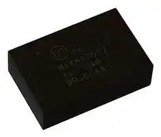


MAXM17546ALY#
DC/DC POL Converter, Adjustable, Buck, Module, 4.5V to 42V In, 0.9V to 12V/5A Out, 2.2MHz, SIP-29
- Manufacturer: ANALOG DEVICES
- Product type: DC / DC Non Isolated Board Mount Converters - Adjustable Output
- DC / DC Converter Type:Module; Input Voltage Min:4.5V; Input Voltage Max:42V; No. of Outputs:1 Output; DC / DC Converter IC Case:SIP; No. of Pins:29Pins; Output Current:5A; Output Voltage M
- MSL: MSL 3 - 168 hours
- SVHC: No SVHC (04-Feb-2026)
- Depth: 9mm
- Width: 15mm
- Height: 4.32mm
- Topology: Synchronous Buck (Step Down)
- No. of Pins: 29Pins
- Product Range: MAXM17546 Series
- No. of Outputs: 1 Output
- Output Current: 5A
- Output Power Max: -
- Input Voltage Max: 42V
- Input Voltage Min: 4.5V
- Output Current Max: 5A
- Output Voltage Max: 12V
- Output Voltage Min: 900mV
- Switching Frequency: 2.2MHz
- Input Voltage DC Max: 42V
- Input Voltage DC Min: 4.5V
- DC / DC Converter Type: SIP-29, Module
- DC / DC Converter IC Case: SIP
- Operating Temperature Max: 125°C
- Power Supply Applications: Industrial
- DC / DC Converter Output Type: Adjustable
| Delivery and price | |
|---|---|
| Units per pack | 132 |
| Price | 13.75 € |
| Current stock | 10+ |
| Lead time | 30 days |
_Click_ _**here** for production status of specific part numbers._

## **MAXM17546**

## **4.5V to 42V, 5A High-Efficiency, DC-DC Step-Down Power Module with Integrated Inductor**

## **General Description**

The Himalaya series of voltage regulator ICs and power modules enable cooler, smaller and simpler power supply solutions. The MAXM17546 is an easy-to-use, step-down power module that combines a switching power supply controller, dual n-channel MOSFET power switches, fully shielded inductor, and the compensation components in a low-profile, thermally-efficient system-in-package (SiP).

The device operates over a wide input voltage range of 4.5V to 42V and delivers up to 5A continuous output current with excellent line and load regulation over an output-voltage range of 0.9V to 12V. The high level of integration significantly reduces design complexity, manufacturing risks, and offers a true plug-and-play power supply solution, reducing time-to-market.

The device can be operated in the pulse-width modulation (PWM), pulse-frequency modulation (PFM), or discontinuous conduction mode (DCM) control schemes.

The MAXM17546 is available in a low-profile, highly thermal-emissive, compact, 29-pin, 9mm x 15mm x 4.32mm SiP package that reduces power dissipation in the package and enhances efficiency. The package is easily soldered onto a printed circuit board and suitable for automated circuit board assembly.

## **Applications**

- Test and Measurement Equipment

- Distributed Supply Regulation

- FPGA and DSP Point-of-Load Regulator

- Base-Station Point-of-Load Regulator

- HVAC and Building Control

## **Benefits and Features**

- Reduces Design Complexity, Manufacturing Risks, and Time-to-Market

   - Integrated Synchronous Step-Down DC-DC Converter

   - Integrated Inductor

   - Integrated FETs

   - Integrated Compensation Components

- Saves Board Space in Space-Constrained Applications

   - Complete Integrated Step-Down Power Supply in a Single Package

   - Small Profile 9mm x 15mm x 4.32mm SiP Package

   - Simplified PCB Design with Minimal External BOM Components

- Offers Flexibility for Power-Design Optimization

   - Wide Input-Voltage Range from 4.5V to 42V

   - Output-Voltage Adjustable Range from 0.9V to 12V

   - Adjustable Frequency with External Frequency Synchronization (100kHz to 2.2MHz)

   - PWM, PFM, or DCM Current-Mode Control

   - Programmable Soft-Start

   - Auxiliary Bootstrap LDO for Improved Efficiency

   - Optional Programmable EN/UVLO

- Operates Reliably in Adverse Industrial Environments

   - Integrated Thermal Protection

   - Hiccup Mode Overload Protection

   - RESET Output-Voltage Monitoring

   - Ambient Operating Temperature Range (-40°C to +125°C) / Junction Temperature Range (-40°C to +150°C)

_**Ordering Information** appears at end of data sheet._

**==> picture [125 x 31] intentionally omitted <==**

_19-100146; Rev 0; 4/18_

## MAXM17546

## 4.5V to 42V, 5A High-Efficiency, DC-DC Step-Down Power Module with Integrated Inductor

## **Typical Application Circuit**

**==> picture [505 x 269] intentionally omitted <==**

**----- Start of picture text -----**<br>
VIN 7.5V TO 42V<br>CIN<br>2 x10µF<br>IN<br>VOUT<br>EN/UVLO OUT<br>R3 VCC MAXM17546 EXTVCC R1  COUT<br>665kΩ  191kΩ<br>DL FB 3 x 22µF<br>RESET BST CF R2<br>LX 2.2pF<br>SS 42.2kΩ<br>CF<br>MODE/SYNC<br>RT<br>SGND PGND<br>CSS<br>22nF<br>CIN:  10µF GRM32ER71H106KA12<br>COUT:  22µF GRM32ER71C226MEA8<br>**----- End of picture text -----**<br>


Maxim Integrated │ 2

www.maximintegrated.com

## MAXM17546

## 4.5V to 42V, 5A High-Efficiency, DC-DC Step-Down Power Module with Integrated Inductor

## **Absolute Maximum Ratings**

IN to PGND ...........................................................-0.3V to +48V EN/UVLO, SS to SGND ........................................-0.3V to +48V LX to PGND................................................-0.3V to (VIN + 0.3V) BST to PGND ........................................................-0.3V to +53V BST to LX .............................................................-0.3V to +6.5V BST to VCC ...........................................................-0.3V to +48V FB, CF, RESET , MODE/SYNC, RT to SGND ......-0.3V to +6.5V DL, VCC to PGND ................................................-0.3V to +6.5V SGND to PGND ....................................................-0.3V to +0.3V

EXTVCC to PGND ................................................-0.3V to +26V OUT to PGND (VIN ≤16V) ..........................-0.3V to (VIN + 0.3V) OUT to PGND (VIN > 16V) ......................................-0.3V to 16V Output Short-Circuit Duration ....................................Continuous Operating Temperature Range  ...........................-40°C to 125°C Junction Temperature (Note 1) ........................................+150°C Storage Temperature Range ...............................-55°C to 150°C Soldering Temperature (reflow) .......................................+240°C

_Stresses beyond those listed under “Absolute Maximum Ratings” may cause permanent damage to the device. These are stress ratings only, and functional operation of the device at these or any other conditions beyond those indicated in the operational sections of the specifications is not implied. Exposure to absolute maximum rating conditions for extended periods may affect device reliability._

## **Package Information**

|**PACKAGE TYPE: 29-PIN SiP**|**PACKAGE TYPE: 29-PIN SiP**|
|---|---|
|Package Code|L29915#1|
|Outline Number|**21-100177**|
|Land Pattern Number|**90-100055**|
|**THERMAL RESISTANCE, FOUR-LAYER BOARD (Note 2)**||
|Junction to Ambient (θJA)|24 ºC/W|


For the latest package outline information and land patterns (footprints), go to **www.maximintegrated.com/packages** . Note that a “+”, “#”, or “-” in the package code indicates RoHS status only. Package drawings may show a different suffix character, but the drawing pertains to the package regardless of RoHS status.

**Note 1:** Junction temperature greater than +125°C degrades operating lifetimes. **Note 2:** Package thermal resistance is measured on an evaluation board with natural convection.

## **Electrical Characteristics**

(VIN = VEN/UVLO = 24V, RRT = OPEN (450kHz), VPGND = VSGND = VMODE/SYNC = 0V, LX = SS = RESET = CF = DL = VCC = OUT = open, VEXTVCC = 0V, VBST to VLX = 5V, VFB = 1V, TA = -40°C to +125°C, unless otherwise noted. Typical values are at TA = +25°C. All voltages are referenced to SGND, unless otherwise noted.) (Note 3)

|**PARAMETER**|**SYMBOL**|**CONDITIONS**|**MIN**<br>**TYP**<br>**MAX**|**UNITS**|
|---|---|---|---|---|
|**INPUT SUPPLY (VIN) **|||||
|Input-Voltage Range|VIN||4.5<br>42|V|
|Input-Shutdown Current|IIN_SH|VEN/UVLO= 0V, (Shutdown mode)|11<br>16|μA|
|Input-Quiescent Current|IQ_PFM|MODE/SYNC = open|128|μA|
||IQ_DCM|DCM Mode|1.27<br>2|mA|
||IQ_PWM|PWM Mode, no load,<br>VOUT= VEXTVCC= 5V|18||
|**ENABLE/UNDERVOLTAGE LOCKOUT (EN/UVLO)**|||||
|EN/UVLO Threshold|VENR|VEN/UVLOrising|1.185<br>1.215<br>1.245|V|
||VENF|VEN/UVLOfalling|1.06<br>1.09<br>1.12||
|Enable Pullup Resistor|RENP|Pullup resistor between IN and<br>EN/UVLO pins|3.15<br>3.32<br>3.45|MΩ|


Maxim Integrated │ 3

www.maximintegrated.com

## MAXM17546

## 4.5V to 42V, 5A High-Efficiency, DC-DC Step-Down Power Module with Integrated Inductor

## **Electrical Characteristics (continued)**

(VIN = VEN/UVLO = 24V, RRT = OPEN (450kHz), VPGND = VSGND = VMODE/SYNC = 0V, LX = SS = RESET = CF = DL = VCC = OUT = open, VEXTVCC = 0V, VBST to VLX = 5V, VFB = 1V, TA = -40°C to +125°C, unless otherwise noted. Typical values are at TA = +25°C. All voltages are referenced to SGND, unless otherwise noted.) (Note 3)

|**PARAMETER**|**SYMBOL**|**CONDITIONS**|**MIN**<br>**TYP**<br>**MAX**|**UNITS**|
|---|---|---|---|---|
|**LOW DROPOUT (INLDO)**|||||
|VCCOutput-Voltage<br>Range|VCC|6V < VIN< 42V, IVCC= 1mA|4.75<br>5<br>5.25|V|
|||1mA < IVCC< 45mA|4.75<br>5<br>5.25||
|VCCCurrent Limit|IVCC_MAX|VCC= 4.3V, VIN= 7V|50<br>90<br>150|mA|
|IN to VCCDropout|VCC_DO|VIN= 4.5V, IVCC= 45mA|0.4|V|
|VCCUVLO|VCC_UVR|VCCrising|4.1<br>4.2<br>4.3|V|
||VCC_UVF|VCCfalling|3.7<br>3.8<br>3.9||
|**LOW DROPOUT (EXTVCC)**|||||
|EXTVCC Operating-<br>Voltage Range|||4.84<br>24|V|
|EXTVCC Switch-Over<br>Voltage||Rising|4.56<br>4.7<br>4.84|V|
|||Falling|4.33<br>4.45<br>4.6||
|EXTVCC to VCCDropout|VEXTVCC_DO|VEXTVCC= 5V, IEXTVCC= 45mA|0.6|V|
|EXTVCC Current Limit|IEXTVCC_MAX|VCC= 4.3V, EXTVCC = 8V|45<br>85<br>140|mA|
|**SOFT-START (SS)**|||||
|Charging Current|ISS|VSS= 0.5V|4.7<br>5<br>5.3|μA|
|**OUTPUT SPECIFICATIONS**|||||
|Line-Regulation Accuracy||VIN= 6.5V to 42V, VOUT= 5V|0.1|mV/V|
|Load-Regulation Accuracy||Tested with IOUT= 0A to 5A at VOUT= 5V|6|mV/A|
|FB-Regulation Voltage|VFB_REG|MODE/SYNC = SGND or MODE = VCC|0.8875<br>0.9<br>0.9135|V|
|||MODE/SYNC = OPEN|0.8875<br>0.915<br>0.936||
|FB Input-Bias Current|IFB|0 < VFB< 1V|-75<br>+75|nA|
|FB Undervoltage Trip Level<br>to Cause Hiccup|VFB_HICF||0.55<br>0.58<br>0.61|V|
|HICCUP Timeout|||32768|Cycles|
|**MODE/SYNC PIN**|||||
|MODE Threshold|VM_DCM|MODE/SYNC = VCC(DCM Mode)|VCC- 0.6|V|
||VM_PFM|MODE/SYNC = OPEN (PFM mode)|VCC/ 2||
||VM_PWM|MODE/SYNC = GND (PWM mode)|0.6||
|SYNC Frequency-<br>Capture Range||fSWset by RRT|1.1 x<br>fSW<br>1.4 x<br>fSW|kHz|
|SYNC Pulse Width|||50|ns|
|SYNC Threshold|VIH||2.0|V|
||VIL||0.8||


Maxim Integrated │ 4

www.maximintegrated.com

## MAXM17546

## 4.5V to 42V, 5A High-Efficiency, DC-DC Step-Down Power Module with Integrated Inductor

## **Electrical Characteristics (continued)**

(VIN = VEN/UVLO = 24V, RRT = OPEN (450kHz), VPGND = VSGND = VMODE/SYNC = 0V, LX = SS = RESET = CF = DL = VCC = OUT = open, VEXTVCC = 0V, VBST to VLX = 5V, VFB = 1V, TA = -40°C to +125°C, unless otherwise noted. Typical values are at TA = +25°C. All voltages are referenced to SGND, unless otherwise noted.) (Note 3)

|**PARAMETER**|**SYMBOL**|**CONDITIONS**|**MIN**<br>**TYP**<br>**MAX**|**UNITS**|
|---|---|---|---|---|
|**CURRENT LIMIT**|||||
|Average Current-Limit<br>Threshold|IAVG_LIMIT||6.75|A|
|**RT PIN**|||||
|Switching Frequency|fSW|RRT= 196KΩ|90<br>100<br>110|kHz|
|||RRT= open|420<br>450<br>480||
|||RRT= 7.5kΩ|1950<br>2200<br>2450||
|Minimum On-Time|tON(MIN)||114<br>160|ns|
|Minimum Of-time|tOFF(MIN)||140<br>160|ns|
|LX Dead Time|tDT||22|ns|
|**RESET PIN**|||||
|RESETOutput-Level Low||IRESET= 10mA|400|mV|
|RESETOutput-Leakage<br>Current||VRESET= 5.5V|-100<br>100|nA|
|VOUTThreshold for<br>RESETAssertion|VOUT_OKF|VFBfalling|90.4<br>92.5<br>94.6|%|
|VOUTThreshold for<br>RESETDeassertion|VOUT_OKR|VFBrising|93.4<br>95.5<br>97.7|%|
|RESETDeassertion Delay<br>after FB Reaches 95%<br>Regulation|||1024|Cycles|
|**THERMAL SHUTDOWN**|||||
|Thermal-Shutdown<br>Threshold||Temperature Rising|165|°C|
|Thermal-Shutdown<br>Hystersis|||10|°C|


**Note 3:** Electrical specifications are production tested at TA = + 25°C. Specifications over the entire operating temperature range are guaranteed by design and characterization.

Maxim Integrated │ 5

www.maximintegrated.com

## MAXM17546

## 4.5V to 42V, 5A High-Efficiency, DC-DC Step-Down

## Power Module with Integrated Inductor

## **Typical Operating Characteristics**

(VIN = VEN/UVLO = 24V, VSGND = VPGND = 0V, TA = -40°C to +125°C, unless otherwise noted. Typical values are at TA = +25°C. All voltages are referenced to GND, unless otherwise noted. The circuit values for different output-voltage applications are as in Table 1, unless otherwise noted.)

**==> picture [651 x 600] intentionally omitted <==**

**----- Start of picture text -----**<br>
EFFICIENCY vs. LOAD CURRENT EFFICIENCY vs. LOAD CURRENT EFFICIENCY vs. LOAD CURRENT<br>(3.3V OUTPUT, PWM MODE, fSW = 400kHz) (5V OUTPUT, PWM MODE, fSW = 450kHz) (3.3V OUTPUT, PFM MODE, fSW = 400kHz)<br>100 toc01 100 toc02 100 toc03<br>90 90 90<br>80 80 80<br>70 70 70<br>VIN = 36V<br>60 60 60<br>50 VIN =  36V 50 VIN = 12V 50<br>40 VIN = 24V 40 VIN = 24V 40 VIN = 36V<br>30 30 30 VIN = 24V<br>VIN = 12V<br>20 20 20 VIN = 12V<br>10 10 10<br>0 1000 2000 3000 4000 5000 0 1000 2000 3000 4000 5000 1 10 100 1000<br>LOAD CURRENT (mA) LOAD CURRENT (mA) LOAD CURRENT (mA)<br>EFFICIENCY vs. LOAD CURRENT EFFICIENCY vs. LOAD CURRENT EFFICIENCY vs. LOAD CURRENT<br>(5V OUTPUT, PFM MODE, fSW = 450kHz) (3.3V OUTPUT, DCM MODE, fSW = 400kHz)  (5V OUTPUT, DCM MODE, fSW = 450kHz)<br>100 toc04 100 toc05 100 toc06<br>90 90 90<br>80 80 VIN = 12V 80<br>70 70 70<br>60 VIN = 36V 60 60 VIN = 36V<br>50 50<br>50 VIN = 12V<br>40 VIN = 36V 40<br>40<br>VIN = 24V 30 30 VIN = 24V<br>30 20 VIN = 24V 20<br>20 10 10 VIN = 12V<br>10 0 0<br>1 10 100 1000 1 10 100 1000 1 10 100 1000<br>LOAD CURRENT (mA) LOAD CURRENT (mA) LOAD CURRENT (mA)<br>EFFICIENCY vs. LOAD CURRENT EFFICIENCY vs. LOAD CURRENT EFFICIENCY vs. LOAD CURRENT<br>(0.9V OUTPUT, PWM MODE, fSW = 300kHz) (1.2V OUTPUT, PWM MODE, fSW = 400kHz)  (1.5V OUTPUT, PWM MODE, fSW = 400kHz)<br>100 toc07 100 toc08 100 toc09<br>90 90 90<br>80 80 80<br>70 70 70<br>60 60 60<br>50 50 50<br>VIN = 12V VIN = 12V<br>40 VIN = 12V 40 40<br>30 VIN = 5V 30 VIN = 5V 30 VIN = 5V<br>20 20 20<br>10 10 10<br>0 1000 2000 3000 4000 5000 0 1000 2000 3000 4000 5000 0 1000 2000 3000 4000 5000<br>LOAD CURRENT (mA) LOAD CURRENT (mA) LOAD CURRENT (mA)<br>www.maximintegrated.com Maxim Integrated │ 6<br>EFFICIENCY (%) EFFICIENCY (%) EFFICIENCY (%)<br>EFFICIENCY (%) EFFICIENCY (%)<br>EFFICIENCY (%)<br>EFFICIENCY (%) EFFICIENCY (%) EFFICIENCY(%)<br>**----- End of picture text -----**<br>


## MAXM17546

## 4.5V to 42V, 5A High-Efficiency, DC-DC Step-Down

## Power Module with Integrated Inductor

## **Typical Operating Characteristics (continued)**

(VIN = VEN/UVLO = 24V, VSGND = VPGND = 0V, TA = -40°C to +125°C, unless otherwise noted. Typical values are at TA = +25°C. All voltages are referenced to GND, unless otherwise noted. The circuit values for different output-voltage applications are as in Table 1, unless otherwise noted.)

**==> picture [653 x 612] intentionally omitted <==**

**----- Start of picture text -----**<br>
EFFICIENCY vs. LOAD CURRENT EFFICIENCY vs. LOAD CURRENT EFFICIENCY vs. LOAD CURRENT<br>(1.8V OUTPUT, PWM MODE, fSW = 400kHz) (2.5V OUTPUT, PWM MODE, fSW = 400kHz) (8V OUTPUT, PWM MODE, fSW = 800kHz)<br>100 toc10 100 toc11 100 toc12<br>90 90 90<br>80 80 80<br>70 VIN = 5V 70 VIN = 5V 70<br>60 60 60 VIN = 36V<br>50 VIN  = 12V 50 VIN = 12V 50 VIN = 12V<br>40 40 40<br>30 VIN = 24V 30 VIN = 24V 30 VIN = 24V<br>20 20 20<br>10 10 10<br>0 1000 2000 3000 4000 5000 0 1000 2000 3000 4000 5000 0 1000 2000 3000 4000 5000<br>LOAD CURRENT (mA) LOAD CURRENT (mA) LOAD CURRENT (mA)<br>EFFICIENCY vs. LOAD CURRENT EFFICIENCY vs. LOAD CURRENT EFFICIENCY vs. LOAD CURRENT<br>(12V OUTPUT, PWM MODE, fSW = 900kHz) (0.9V OUTPUT, PFM MODE, fSW = 300kHz) (1.2V OUTPUT, PFM MODE, fSW = 400kHz)<br>100 toc13 100 toc14 100 toc15<br>90<br>90 90<br>80<br>70 80 80<br>VIN = 36V<br>60<br>70 70<br>50<br>VIN = 12V VIN = 5V<br>40 60 60<br>VIN = 5V<br>30 VIN = 24V 50 50 VIN = 12V<br>20<br>10 40 40<br>0 1000 2000 3000 4000 5000 5 50 500 5000 5 50 500 5000<br>LOAD CURRENT (mA) LOAD CURRENT (mA) LOAD CURRENT (mA)<br>EFFICIENCY vs. LOAD CURRENT EFFICIENCY vs. LOAD CURRENT EFFICIENCY vs. LOAD CURRENT<br>(1.5V OUTPUT, PFM MODE, fSW = 400kHz) (1.8V OUTPUT, PFM MODE, fSW = 400kHz) (2.5V OUTPUT, PFM MODE, fSW = 400kHz)<br>100 toc16 100 toc17 100 toc18<br>90 90 90<br>80 80 80<br>70 70 VIN = 5V 70 VIN = 5V<br>VIN = 5V<br>60 60 VIN = 12V 60 VIN = 12V<br>VIN = 12V VIN = 24V VIN = 24V<br>50 50 50<br>40 40 40<br>5 50 500 5000 5 50 500 5000 5 50 500 5000<br>LOAD CURRENT (mA) LOAD CURRENT (mA) LOAD CURRENT (mA)<br>www.maximintegrated.com Maxim Integrated │ 7<br>EFFICIENCY(%) EFFICIENCY(%) EFFICIENCY (%)<br>EFFICIENCY (%) EFFICIENCY (%)<br>EFFICIENCY (%)<br>EFFICIENCY (%) EFFICIENCY (%) EFFICIENCY (%)<br>**----- End of picture text -----**<br>


## MAXM17546

## 4.5V to 42V, 5A High-Efficiency, DC-DC Step-Down Power Module with Integrated Inductor

## **Typical Operating Characteristics (continued)**

##

(VIN = VEN/UVLO = 24V, VSGND = VPGND = 0V, TA = -40°C to +125°C, unless otherwise noted. Typical values are at TA = +25°C. All voltages are referenced to GND, unless otherwise noted. The circuit values for different output-voltage applications are as in Table 1, unless otherwise noted.)

**==> picture [178 x 513] intentionally omitted <==**

**----- Start of picture text -----**<br>
EFFICIENCY vs. LOAD CURRENT<br>(8V OUTPUT, PFM MODE, fSW = 800kHz)<br>100 toc19<br>90 Ta<br>80 |<br>70 VIN = 36V<br>60 L V ULA IN = 12V T |<br>50 a VIN = 24V Hill<br>40 TT TTT<br>5 50 500 5000<br>LOAD CURRENT (mA)<br>STEADY-STATE SWITCHING WAVEFORMS<br>(VIN = 24V, VOUT = 5V, IOUT = 0A<br>PWM MODE, MODE = SGND)<br>toc21<br>20mV/div<br>VOUT (AC-<br>COUPLED)<br>VLX 10V/div<br>Ll Ln dL<br>2 µ s/div<br>STEADY-STATE SWITCHING WAVEFORMS<br>(VIN = 24V, VOUT = 5V, IOUT = 25mA<br>PFM MODE, MODE = OPEN)<br>toc23<br>100mV/div<br>VOUT (AC-<br>COUPLED)<br>VLX 10V/div<br>100 µ s/div<br>EFFICIENCY (%)<br>**----- End of picture text -----**<br>


**==> picture [176 x 511] intentionally omitted <==**

**----- Start of picture text -----**<br>
EFFICIENCY vs. LOAD CURRENT<br>(12V OUTPUT, PFM MODE, fSW = 900kHz)<br>100 toc20<br>90 TM<br>80 SII<br>70 VIN = 36V<br>60 dNnT |<br>50 ae VIN = 24V<br>40 T TT<br>5 50 500 5000<br>LOAD CURRENT (mA)<br>STEADY-STATE SWITCHING WAVEFORMS<br>(VIN = 24V, VOUT = 5V, IOUT = 5A<br>PWM MODE, MODE = SGND)<br>toc22<br>20mV/div<br>VOUT (AC-<br>COUPLED)<br>VLX 10V/div<br>| ||<br>2 µ s/div<br>STEADY-STATE SWITCHING WAVEFORMS<br>(VIN = 24V, VOUT = 5V, IOUT = 100mA<br>DCM MODE, MODE = VCC)<br>toc24<br>10mV/div<br>VOUT (AC-<br>COUPLED)<br>VLX 10V/div<br>1 µ s/div<br>EFFICIENCY (%)<br>**----- End of picture text -----**<br>


Maxim Integrated │ 8

www.maximintegrated.com

## MAXM17546

## 4.5V to 42V, 5A High-Efficiency, DC-DC Step-Down Power Module with Integrated Inductor

## **Typical Operating Characteristics (continued)**

##

(VIN = VEN/UVLO = 24V, VSGND = VPGND = 0V, TA = -40°C to +125°C, unless otherwise noted. Typical values are at TA = +25°C. All voltages are referenced to GND, unless otherwise noted. The circuit values for different output-voltage applications are as in Table 1, unless otherwise noted.)

**==> picture [421 x 523] intentionally omitted <==**

**----- Start of picture text -----**<br>
OUTPUT VOLTAGE vs. LOAD CURRENT OUTPUT VOLTAGE vs. LOAD CURRENT<br>(5V OUTPUT, PWM MODE, fSW = 450kHz) (5V OUTPUT, PFM MODE, fSW = 450kHz)<br>5.02 toc25 5.20 toc26<br>5.15 EL<br>5.00<br>5.10<br>4.98<br>5.05<br>SUA ROTA Se UT<br>4.96 LAI AAS 5.00 CANAII<br>4.95<br>4.94 VIN = 24V VIN = 12V VIN = 12V<br>CTV 4.90 L ILa<br>4.92 VIN = 42V 4.85 VIN = 42V<br>VIN = 24V<br>4.90 PEE 1 4.80 rte<br>5 50 500 5000 5 50 500 5000<br>LOAD CURRENT (mA) LOAD CURRENT (mA)<br>OUTPUT VOLTAGE vs. LOAD CURRENT OUTPUT VOLTAGE vs. LOAD CURRENT<br>(3.3V OUTPUT, PWM MODE, fSW = 400kHz) (3.3V OUTPUT, PFM MODE, fSW = 400kHz)<br>3.34 toc27 3.45 toc28<br>3.32<br>3.40<br>3.30 S HAE HT SANT<br>3.28 a ARANSOL 3.35 eel iil<br>3.26<br>3.30<br>Bat AN Minn<br>3.24 EL VIN = 24V a| VIN = 12V | VIN = 42V | 3.25 aLL VIN = 24V LL VIN = 12V<br>3.22<br>T T iy CTT VIN = 42V ii<br>3.20 Cl 3.20 UII<br>TI ll<br>5 50 500 5000 5 50 500 5000<br>LOAD CURRENT (mA) LOAD CURRENT (mA)<br>POWER-UP AND DOWN THROUGH EN/UVLO POWER-UP AND DOWN THROUGH EN/UVLO<br>(VIN = 24V, VOUT = 5V, IOUT = 25mA (VIN = 24V, VOUT = 3.3V, IOUT = 25mA<br>PFM MODE, MODE = OPEN) PFM MODE, MODE = OPEN)<br>toc29 toc30<br>VEN/UVLO 2V/div  VEN/UVLO 2V/div<br>VOUT 5V/div VOUT 2V/div<br>VRESET 5V/div VRESET<br>5V/div<br>4ms/div 4ms/div<br>OUTPUT VOLTAGE (V)<br>OUTPUT VOLTAGE (V)<br>OUTPUT VOLTAGE (V) OUTPUT VOLTAGE (V)<br>**----- End of picture text -----**<br>


Maxim Integrated │ 9

www.maximintegrated.com

## MAXM17546

## 4.5V to 42V, 5A High-Efficiency, DC-DC Step-Down Power Module with Integrated Inductor

## **Typical Operating Characteristics (continued)**

(VIN = VEN/UVLO = 24V, VSGND = VPGND = 0V, TA = -40°C to +125°C, unless otherwise noted. Typical values are at TA = +25°C. All voltages are referenced to GND, unless otherwise noted. The circuit values for different output-voltage applications are as in Table 1, unless otherwise noted.)

**==> picture [433 x 516] intentionally omitted <==**

**----- Start of picture text -----**<br>
POWER-UP AND DOWN THROUGH EN/UVLO<br>POWER-UP AND DOWN THROUGH EN/UVLO<br>(VPWM MODE, MODE = SGND)IN = 24V, VOUT = 5V, IOUT = 5A (VPWM MODE, MODE = SGND)IN = 24V, VOUT = 3.3V, IOUT = 5A<br>toc31 toc32<br>VEN/UVLO 2V/div  VEN/UVLO 2V/div<br>VOUT 5V/div VOUT 2V/div<br>VRESET 5V/div VRESET 5V/div<br>IOUT 5A/div IOUT 5A/div<br>4ms/div<br>4ms/div<br>POWER-UP WITH 2.5V BIAS POWER-UP WITH 2.5V BIAS<br>(VIN = 24V, VOUT = 5V, IOUT = 0A (VIN = 24V, VOUT = 3.3V, IOUT = 0A<br>PWM MODE, MODE = SGND) PWM MODE, MODE = SGND)<br>toc33 toc34<br>VEN/UVLO 2V/div  VEN/UVLO 2V/div<br>2V/div 1V/div<br>VOUT VOUT<br>VRESET 5V/div VRESET 5V/div<br>4ms/div 4ms/div<br>LOAD TRANSIENT LOAD TRANSIENT<br>(VIN = 24V, VOUT = 5V, IOUT = 0A TO 2.5A (VIN = 24V, VOUT = 3.3V, IOUT = 0A TO 2.5A<br>PWM MODE, MODE = SGND) PWM MODE, MODE = SGND)<br>toc35 toc36<br>=<br>100mV/div  100mV/div<br>VOUT (AC-COUPLED)  VOUT (AC-COUPLED)<br>1A/div<br>IOUT<br>IOUT 1A/div<br>200 µ s/div 400 µ s/div<br>**----- End of picture text -----**<br>


Maxim Integrated │ 10

www.maximintegrated.com

## MAXM17546

## 4.5V to 42V, 5A High-Efficiency, DC-DC Step-Down Power Module with Integrated Inductor

## **Typical Operating Characteristics (continued)**

(VIN = VEN/UVLO = 24V, VSGND = VPGND = 0V, TA = -40°C to +125°C, unless otherwise noted. Typical values are at TA = +25°C. All voltages are referenced to GND, unless otherwise noted. The circuit values for different output-voltage applications are as in Table 1, unless otherwise noted.)

**==> picture [177 x 514] intentionally omitted <==**

**----- Start of picture text -----**<br>
LOAD TRANSIENT<br>(VIN = 24V, VOUT = 5V, IOUT = 2.5A TO 5A<br>PWM MODE, MODE = SGND)<br>toc37<br>100mV/div<br>VOUT (AC-COUPLED)<br>_povsipnngmininnenni<br>IOUT 2A/div<br>400 µ s/div<br>LOAD TRANSIENT<br>(VIN = 24V, VOUT = 5V, IOUT = 25mA TO 2.5A<br>PFM MODE, MODE = OPEN)<br>toc39<br>100mV/div<br>VOUT (AC-COUPLED)<br>pomenininennenaasesianenatcieietes<br>IOUT 1A/div<br>400 µ s/div<br>LOAD TRANSIENT<br>(VIN = 24V, VOUT = 5V, IOUT = 25mA TO 2.5A<br>DCM MODE, MODE = VCC)<br>toc41<br>100mV/div<br>VOUT (AC-<br>COUPLED)<br>_eimiecnnetnanssaesintemnete erk<br>IOUT 1A/div<br>400 µ s/div<br>**----- End of picture text -----**<br>


**==> picture [171 x 508] intentionally omitted <==**

**----- Start of picture text -----**<br>
LOAD TRANSIENT<br>(VIN = 24V, VOUT = 3.3V, IOUT = 2.5A TO 5A<br>PWM MODE, MODE = SGND) toc38<br>100mV/div<br>VOUT (AC-COUPLED)<br>antares!<br>IOUT 2A/div<br>400 µ s/div<br>LOAD TRANSIENT<br>(VIN = 24V, VOUT = 3.3V, IOUT = 25mA TO 2.5A<br>PFM MODE, MODE = OPEN)<br>toc40<br>100mV/div<br>VOUT (AC-COUPLED)<br>poe nent nme<br>IOUT 1A/div<br>1ms/div<br>LOAD TRANSIENT<br>(VIN = 24V, VOUT = 3.3V, IOUT = 25mA TO 2.5A<br>DCM MODE, MODE = VCC)<br>toc42<br>100mV/div<br>VOUT (AC-COUPLED)<br>ei tentctenentemetet<br>IOUT 1A/div<br>400 µ s/div<br>**----- End of picture text -----**<br>


Maxim Integrated │ 11

www.maximintegrated.com

## MAXM17546

## 4.5V to 42V, 5A High-Efficiency, DC-DC Step-Down Power Module with Integrated Inductor

## **Typical Operating Characteristics (continued)**

(VIN = VEN/UVLO = 24V, VSGND = VPGND = 0V, TA = -40°C to +125°C, unless otherwise noted. Typical values are at TA = +25°C. All voltages are referenced to GND, unless otherwise noted. The circuit values for different output-voltage applications are as in Table 1, unless otherwise noted.)

**==> picture [428 x 537] intentionally omitted <==**

**----- Start of picture text -----**<br>
OUTPUT SHORT IN STEADY STATE STARTUP INTO SHORT<br>(VIN = 24V, VOUT = 5V, OUTPUT SHORT (VIN = 24V, VOUT = 5V, OUTPUT SHORT<br>PWM MODE, MODE = SGND) PWM MODE, MODE = SGND)<br>toc43 toc44<br>VOUT 500mV/div  VEN/UVLO 2V/div<br>VOUT 500mV/div<br>VLX 20V/div  VLX 20V/div<br>ae<br>IOUT 5A/div IOUT 5A/div<br>| ao<br>20ms/div 2ms/div<br>SYNC FREQUENCY AT 630kHz<br>(VIN = 24V, VOUT = 5V, IOUT = 5A BODE PLOT<br>PWM MODE, MODE = SGND)<br>toc45 40 (VIN = 24V, VOUT = 5V, IOUT = 5A) toc46 120<br>30 PHASE 100<br>80<br>20<br>VSYNC ilWEl| ||| 2V/div  10 eeeSSS COTMT 60<br>OTST<br>40<br>0 TTT SN<br>20<br>-10 GAIN<br>0<br>Sporn -20 en Ta<br>VLX 10V/div  fCR = 36kHz,  -20<br>ENE) 2 µ s/div -30-40 nTeen PHASE MARGIN = 62 ° mall -40-60<br>10 [3] 10 [4] 10 [5]<br>FREQUENCY (Hz)<br>BODE PLOT<br>OUTPUT CURRENT<br>(VIN = 24V, VOUT = 3.3V, IOUT = 5A) vs. AMBIENT TEMPERATURE<br>40 toc47 120 6 toc48<br>30 LL M PHASE 100<br>5<br>80<br>20<br>SECT TTI 60 4 5<br>10<br>a sl 40 \<br>0 CUTIE SSC 3 po VOUT = 5V<br>20<br>-10 GAIN<br>0 2<br>-20 -20 VOUT = 3.3V<br>-30 an fPHASE MARGIN = 63CR = 39kHz,  it ° -40 1 ca aea y<br>-40 eeeeenalianil -60 0 |Ft ||| tt i\<br>10 [3] 10 [4] 10 [5] 0 20 40 60 80 100 120<br>FREQUENCY(Hz) AMBIENT TEMPERATURE ( ° C)<br>GAIN (dB) ) ° PHASE (<br>GAIN (dB) ) ° PHASE (<br>OUTPUT CURRENT (A)<br>**----- End of picture text -----**<br>


Maxim Integrated │ 12

www.maximintegrated.com

## MAXM17546

## 4.5V to 42V, 5A High-Efficiency, DC-DC Step-Down Power Module with Integrated Inductor

## **Pin Configuration**

**==> picture [505 x 331] intentionally omitted <==**

**----- Start of picture text -----**<br>
MODE/SYNC IN PGND DL OUT OUT<br>+<br>VCC 1 29 28 27 26 25 23 OUT<br>24<br>RESET 2 MAXM17546 22 OUT<br>RT 3 21 PGND<br>EP1 EP2<br>SGND 4 20 PGND<br>CF 5 19 PGND<br>EP3<br>FB 6 18<br>PGND<br>7 8 9 10 11 12 13 14 15 16 17 PGND<br>SS EN/UVLO IN PGND EXTVCC BST LX PGND PGND PGND<br>9mm x 15mm x 4.32mm 29-PIN SiP<br>**----- End of picture text -----**<br>


## **Pin Description**

|**PIN**|**NAME**|**FUNCTION**|
|---|---|---|
|1|VCC|5V LDO Output. The VCCis bypassed to PGND internally through a 2.2µF capacitor. Do not con-<br>nect any external components to the VCCpin.|
|2|RESET|Open-DrainRESETOutput. TheRESEToutput is driven low if FB drops below 92% of its set<br>value.RESETgoes high 1024 clock cycles after FB rises above 95% of its set value.|
|3|RT|Switching Frequency Programming Pin. Connect a resistor from RT to SGND to set the<br>regulator's switching frequency. Leave RT open for the default 450kHz frequency.|
|4|SGND|Analog Ground.|
|5|CF|Compensation Pin. Connect a 2.2pF capacitor from CF to FB.|
|6|FB|Feedback Input. Connect FB to the center tap of an external resistor-divider from the OUT to<br>SGND to set the output voltage.|
|7|SS|Soft-Start Input. Connect a capacitor from SS to SGND to set the soft-start time.|
|8|EN/UVLO|Enable/Undervoltage-Lockout Input. Connect a resistor from EN/UVLO to SGND to set the UVLO<br>threshold. By default, the module is enabled with the EN/UVLO pin open.|


Maxim Integrated │ 13

www.maximintegrated.com

## MAXM17546

## 4.5V to 42V, 5A High-Efficiency, DC-DC Step-Down Power Module with Integrated Inductor

## **Pin Description (continued)**

|**PIN**|**NAME**|**FUNCTION**|
|---|---|---|
|9, 28|IN|Power-Supply Input. Decouple to PGND with a capacitor; place the capacitor close to the<br>IN and PGND pins.|
|10,<br>14-21, 27|PGND|Power Ground|
|11|EXTVCC|External Power Supply Input for the Internal LDO. Applying a voltage between 4.7V and 24V at<br>the EXTVCC pin bypasses the internal LDO and improves efciency.|
|12|BST|Boost Flying Capacitor Node. Internally a 0.1μF is connected from BST to LX. Do not connect any<br>external components to the BST pin.|
|13|LX|Switching Node. Leave unconnected; do not connect any external components to the LX pin.|
|22-25|OUT|Regulator Output Pin. Connect a capacitor from OUT to PGND.|
|26|DL|Gate Drive for Low-Side MOSFET. Do not connect any external components to the DL pin.|
|29|MODE/SYNC|MODE Pin Confgures the Part to Operate in PWM, PFM, or DCM Modes of Operation.<br>Leave MODE unconnected for PFM operation (pulse skipping at light loads). Connect MODE<br>to SGND for constant frequency PWM operation at all loads. Connect MODE to VCCfor DCM<br>operation. The device can be synchronized to an external clock using this pin.<br>See the_MODE/SYNC setting_section for more details.|
|EP1, EP2,<br>EP3|—|Exposed Pad. Create a large copper plane below the module connecting EP1, EP2, and<br>EP3 to improve heat dissipation capability. PGND and SGND are shorted through this plane.|


Maxim Integrated │ 14

www.maximintegrated.com

## MAXM17546

## 4.5V to 42V, 5A High-Efficiency, DC-DC Step-Down Power Module with Integrated Inductor

## **Functional Diagrams Internal Diagram**

**==> picture [506 x 549] intentionally omitted <==**

**----- Start of picture text -----**<br>
MAXM17546<br>IN<br>VCC LDO<br>SELECT 1µF 1µF<br>2.2µF<br>INLDO<br>EXTVCC<br>BST<br>4.7Ω LDO 3.32MΩ<br>0.1µF 0.1µF<br>SGND CURRENT- SENSE LX<br>LOGIC<br>PEAK<br>EN/UVLO CURRENT- 4.7µH<br>OUT<br>MODE<br>CONTROLLER<br>1.215V 0.22µF<br>HICCUP<br>RT 4.7Ω PGND<br>OSCILLATOR<br>DL<br>CF<br>FB<br>ERROR AMPLIFIER/  MODE-SELECTION<br>MODE/<br>LOOP COMPENSATION LOGIC<br>SYNC<br>SLOPE<br>VCC COMPENSATION<br>SWITCHOVER<br>LOGIC<br>RESET<br>5μA<br>SS<br>FB<br>HICCUP RESET<br>LOGIC<br>EN/UVLO<br>**----- End of picture text -----**<br>


Maxim Integrated │ 15

www.maximintegrated.com

## MAXM17546

## 4.5V to 42V, 5A High-Efficiency, DC-DC Step-Down Power Module with Integrated Inductor

## **Detailed Description**

The MAXM17546 is a high-efficiency, high-voltage, synchronous step-down module with dual-integrated MOSFETs that operates over a 4.5V to 42V input, and supports a programmable output voltage from 0.9V to 12V, delivering up to 5A current. Built-in compensation for the entire output-voltage range eliminates the need for external components. The feedback (FB) regulation accuracy over -40°C to +125°C is ±1.5%.

The device features a peak-current-mode control architecture. An internal transconductance-error amplifier produces an integrated error voltage at an internal node that sets the duty cycle using a PWM comparator, a highside current-sense amplifier, and a slope-compensation generator. At each rising edge of the clock, the high-side MOSFET turns on and remains on until either the appropriate or maximum duty cycle is reached, or the peak current limit is detected. During the high-side MOSFET’s on-time, the inductor current ramps up. During the second half of the switching cycle, the high-side MOSFET turns off and the low-side MOSFET turns on. The inductor releases the stored energy as its current ramps down and provides current to the output. The device features a MODE/SYNC pin that can be used to operate the device in PWM, PFM, or DCM control schemes and to synchronize the switching frequency to an external clock. The device integrates adjustable-input undervoltage lockout, adjustable soft-start, open-drain RESET , auxiliary bootstrap LDO, and DL-to-LX short-detection features.

## **Mode Selection (MODE)**

The logic state of the MODE/SYNC pin is latched when VCC and EN/UVLO voltages exceed the respective UVLO rising thresholds and all internal voltages are ready to allow LX switching. If the MODE/SYNC pin is open at power-up, the device operates in PFM mode at light loads. If the MODE/SYNC pin is grounded at power-up, the device operates in constant-frequency PWM mode at all loads. Finally, if the MODE/SYNC pin is connected to VCC at power-up, the device operates in constant frequency DCM mode at light loads. State changes on the MODE/SYNC pin are ignored during normal operation.

## **PWM-Mode Operation**

In PWM mode, the inductor current is allowed to go negative. PWM operation provides constant frequency operation at all loads, and is useful in applications sensitive to changes in switching frequency. However, the PWM mode of operation gives lower efficiency at light loads compared to PFM and DCM modes of operation.

## **PFM-Mode Operation**

The PFM mode of operation disables negative inductor current and additionally skips pulses at light loads for high efficiency. In PFM mode, the inductor current is forced to a fixed peak of 2A (typ) every clock cycle until the output rises to 102.3% of the nominal voltage. Once the output reaches 102.3% of the nominal voltage, both the highside and low-side FETs are turned off and the device enters hibernate operation until the load discharges the output to 101.1% of the nominal voltage. Most of the internal blocks are turned off in hibernate operation to minimize quiescent current. After the output falls below 101.1% of the nominal voltage, the device comes out of hibernate operation, turns on all internal blocks, and again commences the process of delivering pulses of energy to the output until it reaches 102.3% of the nominal output voltage. The advantage of the PFM mode is higher efficiency at light loads because of lower quiescent current drawn from the supply. The disadvantage is that the output-voltage ripple is higher compared to PWM or DCM modes of operation and switching frequency is not constant at light loads.

## **DCM-Mode Operation**

DCM mode of operation features constant frequency operation down to lighter loads than PFM mode, by not skipping pulses but only disabling negative inductor current at light loads. DCM operation offers efficiency performance that lies between PWM and PFM modes

## **Linear Regulator**

The MAXM17546 has two internal low-dropout (LDO) regulators that powers VCC. During power-up, when the EN/UVLO pin voltage is above the true shutdown voltage, then the VCC is powered from INLDO. When VCC voltage is above the VCC UVLO threshold and EXTVCC voltage is greater than 4.7V (typ) the VCC is powered from EXTVCC LDO. Only one of the two LDOs is in operation at a time depending on the voltage level present at EXTVCC. Powering VCC from EXTVCC increases efficiency at higher input voltages. EXTVCC voltage should not exceed 24V.

Typical VCC output voltage is 5V. Internally VCC is bypassed with a 2.2μF ceramic capacitor to PGND. See the _Electrical Characteristics_ table for the current limit details for both the regulators. In applications where the buck converter output is connected to the EXTVCC pin, if the output is shorted to ground, then the transfer from EXTVCC LDO to INLDO happens seamlessly without any impact on the normal functionality.

Maxim Integrated │ 16

www.maximintegrated.com

## MAXM17546

## 4.5V to 42V, 5A High-Efficiency, DC-DC Step-Down Power Module with Integrated Inductor

## **Setting the Switching Frequency (RT)**

The switching frequency of the MAXM17546 can be programmed from 100kHz to 2.2MHz by using a resistor connected from RT to SGND. The switching frequency (fSW) is related to the resistor connected at the RT pin (RRT) by the following equation:

**==> picture [92 x 27] intentionally omitted <==**

where RRT is in kΩ and fSW is in kHz. Leaving the RT pin open causes the device to operate at the default switching frequency of 450kHz. See the _Electrical Characteristics_ table for RT resistor value recommendations for a few common frequencies.

## **Operating Input-Voltage Range**

The minimum and maximum operating input voltages for a given output voltage should be calculated as follows:

**==> picture [233 x 63] intentionally omitted <==**

where VOUT is the steady-state output voltage, IOUT(MAX) is the maximum load current, fSW(MAX) is the maximum switching frequency, tOFF(MAX) is the worst-case minimum switch off-time (160ns), and tON(MIN) is the worstcase minimum switch on-time (160ns).

The _Component Selection Table_ , Table 1 provides the operating input-voltage range and the optimum switchingfrequency range for the different selected output voltages.

## **External Frequency Synchronization**

The internal oscillator of the MAXM17546 can be synchronized to an external clock signal on the MODE/SYNC pin. The external synchronization clock frequency must be between 1.1 x fSW and 1.4 x fSW, where fSW is the frequency programmed by the RT resistor. When an external clock is applied to the MODE/SYNC pin, the internal oscillator frequency changes to the external clock frequency (from the original frequency based on the RT setting) after detecting 16 external clock edges. The converter operates in PWM mode during synchronization operation. When the external clock is applied to the MODE/SYNC pin, the mode of operation changes to PWM from the initial state

of PFM/DCM. When the external clock is removed on-fly then the internal oscillator frequency changes to the RT set frequency and the converter still continues to operate in PWM mode. The minimum external clock pulse-width high should be greater than 50ns. See the _MODE/SYNC_ section in the _Electrical Characteristics_ table for details.

## **DL-to-OUT Short Detection**

In MAXM17546, DL and OUT pins are adjacent to each other. To prevent damage to the low-side FET in case the DL pin is shorted to the OUT pins, the DL-to-OUT short detection feature has been implemented. If the MAXM17546 detects that the DL pin is shorted to the OUT pins before startup, the startup sequence is not initiated and output voltage is not soft-started.

## **Overcurrent-Protection/HICCUP Mode**

The MAXM17546 is provided with a robust overcurrent protection scheme that protects the device under overload and output short-circuit conditions. If output voltage drops to 68% (typ) of its nominal value any time after soft-start is complete, hiccup mode is triggered. In addition, one occurrence of peak inductor current exceeding the 8.8A (typ) level triggers a hiccup mode. In hiccup mode, the converter is protected by suspending switching for a hiccup timeout period of 32768 clock cycles. Once the hiccup timeout period expires, soft-start is attempted again.

## **RESET Output**

The MAXM17546 includes a  comparator to monitor the output voltage. The open-drain RESET output requires an external pullup resistor. RESET goes high (high impedance) 1024 switching cycles after the regulator output increases above 95.5% of the designed nominal regulated voltage. RESET goes low when the regulator output voltage drops to below 92.5% of the nominal regulated voltage. RESET also goes low during thermal shutdown.

## **Prebiased Output**

When the MAXM17546 starts into a prebiased output, both the high-side and the low-side switches are turned off so that the converter does not sink current from the output. High-side and low-side switches do not start switching until the PWM comparator commands the first PWM pulse, at which point switching commences. The output voltage is then smoothly ramped up to the target value in alignment with the internal reference.

Maxim Integrated │ 17

www.maximintegrated.com

## MAXM17546

## 4.5V to 42V, 5A High-Efficiency, DC-DC Step-Down Power Module with Integrated Inductor

## **Thermal-Shutdown Protection**

Thermal shutdown protection limits total power dissipation in the MAXM17546. When the junction temperature of the device exceeds +165°C (typ), an on-chip thermal sensor shuts down the device, allowing the device to cool. The thermal sensor turns the device on again after the junction temperature cools by 10°C. Soft-start resets during thermal shutdown. Carefully evaluate the total power dissipation (see the _Power Dissipation_ section) to avoid unwanted triggering of the thermal shutdown in normal operation.

## **Applications Information**

## **Input-Capacitor Selection**

The input-filter capacitor reduces peak currents drawn from the power source and reduces noise and voltage ripple on the input caused by the circuit’s switching. The input capacitor RMS current requirement (IRMS) is defined by the following equation:

**==> picture [196 x 30] intentionally omitted <==**

where, IOUT(MAX) is the maximum load current. IRMS has a maximum value when the input voltage equals twice the output voltage (VIN = 2 x VOUT), so IRMS(MAX) = IOUT(MAX)/2. Choose an input capacitor that exhibits less than a +10°C temperature rise at the RMS input current for optimal long-term reliability. Use low-ESR ceramic capacitors with high ripple-current capability at the input. X7R capacitors are recommended in industrial applications for their temperature stability. The CIN capacitor values in Table 1 are the minimum recommended values for the associated operating conditions.

In applications where the source is located distant from the MAXM17546 input, an electrolytic capacitor should be added in parallel to the ceramic capacitor to provide necessary damping for potential oscillations caused by the inductance of the longer input power path and input ceramic capacitor.

## **Output-Capacitor Selection**

X7R ceramic output capacitors are preferred due to their stability over temperature in industrial applications. The output capacitors are usually sized to support a step load of 50% of the maximum output current in the application, so the output-voltage deviation is contained to 3% of the output-voltage change. The minimum required output capacitance can be calculated as follows:

**==> picture [145 x 61] intentionally omitted <==**

where:

ISTEP = Load-current step,

tRESPONSE = Response time of the controller,

VOUT = Allowable output-voltage deviation,

fC = Target closed-loop crossover frequency,

fSW = Switching frequency.Select fC to be 1/10th of fSW if the swtiching frequency is less than or equal to 400kHz. Select fC to be 40kHz if the switching frequency is more than 400kHz.

## **Soft-Start Capacitor Selection**

The MAXM17546 implements adjustable soft-start operation to reduce inrush current. A capacitor connected from the SS pin to SGND programs the soft-start time. The selected output capacitance (CSEL) and the output voltage (VOUT) determine the minimum required soft-start capacitor as follows:

**==> picture [142 x 14] intentionally omitted <==**

The soft-start time (tSS) is related to the capacitor connected at SS (CSS) by the following equation:

**==> picture [51 x 23] intentionally omitted <==**

where tSS is in milliseconds and CSS is in nanofarads. For example, to program a 4ms soft-start time, a 22nF capacitor should be connected from the SS pin to SGND.

Maxim Integrated │ 18

www.maximintegrated.com

## MAXM17546

## 4.5V to 42V, 5A High-Efficiency, DC-DC Step-Down Power Module with Integrated Inductor

## **Setting the Input Undervoltage-Lockout Level**

The MAXM17546 offers an adjustable input undervoltage lockout level. Set the voltage at which MAXM17546 turns on. Calculate R3 as follows:

**==> picture [86 x 26] intentionally omitted <==**

where R3 is in MΩ and VINU is the voltage at which the MAXM17546 is required to turn on. Ensure that VINU is higher than 0.8 x VOUT.

## **Loop Compensation**

The MAXM17546 is internally loop-compensated. Connect a 2.2pF capacitor from CF to FB for stable operation.

Typically, designs with crossover frequency (fC) less than fSW/10 and less than 40kHz offers good phase margin and transient response. For other choices of fC, the design should be carefully evaluated according to user requirements.

**==> picture [242 x 138] intentionally omitted <==**

**----- Start of picture text -----**<br>
IN<br>MAXM17546<br>EN/UVLO<br>R3<br>SGND<br>**----- End of picture text -----**<br>


_Figure 1. Setting the Input-Undervoltage Lockout_

## **Adjusting Output Voltage**

Set the output voltage with a resistive voltage-divider connected from the positive terminal of the output capacitor (VOUT) to SGND (see Figure 2). Connect the center node of the divider to the FB pin. To choose the resistive voltage-divider values calculate for resistor R1, then R2.

First, calculate resistor R1 from the output to FB as follows:

**==> picture [71 x 28] intentionally omitted <==**

where:

R1 is in kΩ

fC = Desired crossover frequency (kHz)

COUT = Derated value of the capacitor due to DC bias (µF) Then, calculate resistor R2 from FB to SGND as follows:

**==> picture [242 x 176] intentionally omitted <==**

**----- Start of picture text -----**<br>
R1× 0.9<br>R2 =<br>(VOUT − 0.9)<br>VOUT<br>MAXM17546<br>R1<br>FB<br>R2<br>SGND<br>**----- End of picture text -----**<br>


_Figure 2. Setting the Output Voltage_

## **Component Selection Table**

**Table 1. Selection Component Values**

|**VIN (V)**|**VOUT (V)**|**CIN**|**COUT**|**R1 (kΩ)**|**R2 (kΩ)**|**fSW (kHz)**|**RRT (kΩ)**|
|---|---|---|---|---|---|---|---|
|4.5 to 16|0.9|2 x 10μF, 1210, X7R, 50V|12 x 47μF, 1210, X7R, 6.3V|33.2|Open|300|61.9|
|4.5 to 17|1.2|2 x 10μF, 1210, X7R, 50V|9 x 47μF, 1210, X7R, 6.3V|39.2|118|400|45.3|
|4.5 to 21|1.5|2 x 10μF, 1210, X7R, 50V|7 x 47μF, 1210, X7R, 6.3V|52.3|78.7|400|45.3|
|4.5 to 26|1.8|2 x 10μF, 1210, X7R, 50V|5 x 47μF, 1210, X7R, 6.3V|71.5|71.5|400|45.3|
|4.5 to 35|2.5|2 x 10μF, 1210, X7R, 50V|4 x 47μF, 1210, X7R, 6.3V|71.5|40.2|400|45.3|
|4.5 to 42|3.3|2 x 10μF, 1210, X7R, 100V|3 x 47μF, 1210, X7R, 10V|158|59|400|45.3|
|7.5 to 42|5|2 x 10μF, 1210, X7R, 100V|3 x 22μF, 1210, X7R, 10V|191|42.2|450|Open|
|10 to 42|8|2 x 10μF, 1210, X7R, 100V|3 x 22μF, 1210, X7R, 16V|232|29.4|800|22.1|
|18 to 42|12|2 x 10μF, 1210, X7R, 100V|2 x 22μF, 1210, X7R, 16V|340|27.4|900|19.6|


Maxim Integrated │ 19

www.maximintegrated.com

## MAXM17546

## 4.5V to 42V, 5A High-Efficiency, DC-DC Step-Down Power Module with Integrated Inductor

## **Power Dissipation**

Ensure that the junction temperature of the MAXM17546 does not exceed +125°C under the operating conditions specified for the power supply. At a given operating condition, the power losses that lead to temperature rise of the part are estimated as follows:

**==> picture [168 x 66] intentionally omitted <==**

where,

POUT = Total output power,

η = Efficiency of the converter,

VOUT = Output voltage,

VIN = Input voltage,

TA = Operating temperature

For the MAXM17546 EV kit, the thermal performance metrics for the package is given below:

## **PCB Layout Guidelines**

- All connections carrying pulsed currents must be very short and as wide as possible. The inductance of these connections must be kept to an absolute minimum due to the high di/dt of the currents. Since inductance of a current carrying loop is proportional to the area enclosed by the loop, if the loop area is made very small, inductance is reduced. Additionally, small current-loop areas reduce radiated EMI.

- A ceramic input-filter capacitor should be placed close to the IN pins of the module. This eliminates as much trace-inductance effects as possible and gives the module a cleaner voltage supply.

- PCB layout also affects the thermal performance of the design. A number of thermal vias that connect to a large ground plane should be provided under the exposed pad of the part, for efficient heat dissipation.

- For a sample layout that ensures first pass success, refer to the MAXM17546 evaluation kit PCB layout available at www.maximintegrated.com.

## θJA = 24°C/W

The junction temperature of the MAXM17546 can be estimated at any given ambient temperature (TA) from the equation below:

TJ(MAX ) = TA + (θ JA × PLOSS )

Maxim Integrated │ 20

www.maximintegrated.com

## MAXM17546

## 4.5V to 42V, 5A High-Efficiency, DC-DC Step-Down Power Module with Integrated Inductor

## **Typical Application Circuits**

## **Typical Application Circuit 5V Output**

**==> picture [504 x 255] intentionally omitted <==**

**----- Start of picture text -----**<br>
VIN 7.5V TO 42V<br>C1 C2<br>10µF 10µF<br>IN<br>VOUT 5V, 5A<br>EN/UVLO OUT<br>MAXM17546 R1 = 191kΩ<br>VCC EXTVCC<br>R3 = 665kΩ<br>FB C3 C4 C5<br>DL BST CF R2 = 42.2kΩ  22µF 22µF 22µF<br>RESET<br>LX<br>2.2pF<br>SS<br>CF<br>MODE/SYNC<br>RT<br>CSS = 22nF SGND PGND<br>C1, C2: GRM32ER71H106KA12<br>C3, C4, C5: GRM32ER71C226MEA8<br>**----- End of picture text -----**<br>


## **Typical Application Circuit 3.3V**

**==> picture [504 x 258] intentionally omitted <==**

**----- Start of picture text -----**<br>
VIN 4.5V TO 42V<br>C1 C2<br>10µF 10µF<br>IN<br>VOUT 3.3V, 5A<br>EN/UVLO OUT<br>MAXM17546<br>VCC R1 = 158kΩ<br>FB C3 C4 C5<br>DL 47µF 47µF 47µF<br>BST CF<br>RESET<br>LX R2 = 59kΩ<br>2.2pF<br>SS<br>CF<br>MODE/SYNC<br>RT<br>CSS = 22nF SGND EXTVCC PGND<br>R4 = 45.3kΩ<br>C1, C2: GRM32ER71H106KA12<br>C3, C4, C5: GRM32ER70J476KE20L<br>**----- End of picture text -----**<br>


Maxim Integrated │ 21

www.maximintegrated.com

## MAXM17546

## 4.5V to 42V, 5A High-Efficiency, DC-DC Step-Down Power Module with Integrated Inductor

## **Ordering Information**

|**PART NUMBER**|**TEMP RANGE**|**PIN-PACKAGE**|
|---|---|---|
|MAXM17546ALY#|-40°C to +125°C|29-pin SiP|
|MAXM17546ALY#T|-40°C to +125°C|29-pin SiP|


_#Denotes a RoHS-compliant device that may include lead(Pb) that is exempt under the RoHS requirements. T = Tape and reel._

Maxim Integrated │ 22

www.maximintegrated.com

## MAXM17546

## 4.5V to 42V, 5A High-Efficiency, DC-DC Step-Down Power Module with Integrated Inductor

## **Revision History**

|**Revision**|**History**|||
|---|---|---|---|
|**REVISION**<br>**NUMBER**|**REVISION**<br>**DATE**|**DESCRIPTION**|**PAGES**<br>**CHANGED**|
|0|4/18|Initial release|—|


For pricing, delivery, and ordering information, please contact Maxim Direct at 1-888-629-4642, or visit Maxim Integrated’s website at www.maximintegrated.com.

_Maxim Integrated cannot assume responsibility for use of any circuitry other than circuitry entirely embodied in a Maxim Integrated product. No circuit patent licenses are implied. Maxim Integrated reserves the right to change the circuitry and specifications without notice at any time. The parametric values (min and max limits) shown in the Electrical Characteristics table are guaranteed. Other parametric values quoted in this data sheet are provided for guidance._

© 2018 Maxim Integrated Products, Inc. │ 23

Maxim Integrated and the Maxim Integrated logo are trademarks of Maxim Integrated Products, Inc.
Updated at April 10, 2026
Since its inception in 1965, Analog Devices has established itself as a global leader in the design and manufacturing of high-performance analog, mixed-signal, and digital signal processing (DSP) integrated circuits. The company is renowned for solving complex engineering challenges by providing critical technologies that seamlessly convert real-world phenomena into precise electrical signals for the industrial, automotive, communications, and consumer markets. Within its extensive portfolio, Analog Devices provides highly reliable clock, timing, and frequency management solutions, featuring a comprehensive array of precision timers, oscillators, and pulse generators. Complementing this core lineup is a robust offering of driver and interface ICs, particularly high-performance I/O expanders that enable seamless connectivity and streamline complex electronic system architectures. Beyond these foundational integrated circuits, Analog Devices leads the industry in sensor innovation, delivering advanced MEMS accelerometers and integrated MEMS modules designed for exceptional precision in motion sensing. To support complete hardware designs, the company's specialized offerings also encompass discrete bipolar transistors, sub-2.4GHz RF transceivers, temperature-compensated oscillators, and dedicated power management components such as DC/DC converters and LED driver ICs.
About Novapart
Novapart is a B2B electronic component broker specialising in stock shortages and cost reduction. We source hard-to-find parts and identify compliant alternatives across a catalogue of 410,000+ components from 500+ manufacturers.
Learn more →Stock Shortage Specialist
When a component is unavailable, discontinued or has an unacceptable lead time, we tap into our network of vetted European and Asian distributors to source what you need — without compromising on quality or traceability.
Request a quote →Compliant Alternatives
We identify pin-to-pin, electrically equivalent substitutes that meet the same certifications (RoHS, AEC-Q100, REACH) as your original specification — validated against datasheets, not just part numbers. Often at a lower cost.
BOM Analysis service →