
Image not available
Illustrative purposes only

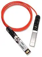
AFBR-2CAR01Z
ACTIVE OPTICAL CABLE, SFP+, 10GBE, 1M
⚠️ Reference pricing provided. In case of supply shortages, we will connect you with our trusted procurement partners to ensure your project's continuity.
- Manufacturer: FOXCONN
- Product type: Fiber Optic Lead Assemblies
- Fibre Type: Multimode
- No. of Fibres: 2Fibres
- Product Range: AFBR
- Fibre Diameter: 62.5µm / 125µm
- External Diameter: 3mm
- Lead Length - Metric: 1m
| Delivery and price | |
|---|---|
| Units per pack | 1 |
| Price | 47.97 € |
| Current stock | 10+ |
| Lead time | 30 days |
Datasheet

## **AFBR-2CARxxZ** 10G Ethernet SFP+ Active Optical Cable (AOC)

## **Data Sheet**

## **Description**

The Avago Technologies’ AFBR-2CARxxZ Active Optical Cable (AOC) is part of a family of SFP+ products to serve 10Gb Ethernet (10GbE) applications.  The letters “xx” of the part number AFBR-2CARxxZ denoted the cable length in meters.  The AFBR-2CARxxZ AOC enables 10GbE equipment designs with very high port density based on the new electrical and mechanical specification enhancements to the well known SFP specifications developed by the SFF Committee. The specifications are referred to as “SFP+” to represent the enhancements over previous SFP specifications. The SFP+ AOC have a cable length up to 20m.  These AOCs can be used as an alternative solution to SFP+ passive and active copper cables, while providing improved signal integrity, longer distances, superior electromagnetic immunity and better bit error rate performance.

## **Related Products**

- The AFBR-703SDZ (AFBR-703ASDZ) is an SFP+ 10 Gigabit Ethernet 10GBASE-SR transceiver with case temperature operated at  0-70 (0-85) °C for use on multimode fiber cables. It is best suited for OM3 high bandwidth MMF link applications with link lengths up to 300 meters.

- AFBR-707SDZ SFP+ 10 Gigabit Ethernet 10GBASELRM transceiver for 220 meter operation in all MMF link applications including OM1 and OM2 legacy fiber cables and new high bandwidth OM3 fiber cables.

- The AFBR-704SDZ is an SFP+ transceiver for 10GbE 10GBASE-USR applications with case temperature 0-70 °C for use on multimode fiber cables up to 100m.

- AFCT-5016Z SFP+ Evaluation Board The purpose of this SFP+ evaluation board is to provide the designer with a convenient means for evaluating SFP+ fiber optic transceivers.

## **Features**

- Proven High Reliability 850 nm technology: Avago VCSEL transmitter and Avago PIN receiver

- Maximum power dissipation 350mW per Active Cable end

- Avago SFP+ package design enables equipment EMI performance in high port density applications with margin to Class B limits

## **Specifications**

- Electrical specifications per SFF-8431 Specifications for Enhanced Small Form Factor Pluggable Module SFP+

- 0 to 70°C case temperature operating range

- Rx_LOS and Tx_DISABLE supported

- Mechanical specifications per SFF Committee SFF 8432 Improved Pluggable Formfactor “IPF”

- Compliant to Restriction on Hazardous Substances (RoHS) per EU and China requirements

- Class 1 eye safe per requirement of EN 60825-1 2007, EN 60825-2 A2 2010

- 1E-15 BER performance

## **Applications**

- 1/10 Gigabit Ethernet (1/10GbE)

- 1/2/4/8G Fibre Channel (1/2/4/8GFC), Fibre Channel over Ethernet (FCoE)

- InfiniBand (QDR/DDR/SDR)

- Data Center Networking

   - Converged Enhanced Ethernet Data Centers

   - Data Center Bridging

- Networked storage systems

- High Performance Computing

- Proprietary Interconnects

Patent - www.avagotech.com/patents

|**Part Number**|**Description**|
|---|---|
|AFBR-2CAR01Z|1 meter SFP+ Active Optical Cable|
|AFBR-2CAR02Z|2 meter SFP+ Active Optical Cable|
|AFBR-2CAR03Z|3 meter SFP+ Active Optical Cable|
|AFBR-2CAR05Z|5 meter SFP+ Active Optical Cable|
|AFBR-2CAR07Z|7 meter SFP+ Active Optical Cable|
|AFBR-2CAR10Z|10 meter SFP+ Active Optical Cable|
|AFBR-2CAR15Z|15 meter SFP+ Active Optical Cable|
|AFBR-2CAR20Z|20 meter SFP+ Active Optical Cable|
|AFCT-5016Z|SFP+ Evaluation Board|


## **Installation**

The AFBR-2CARxxZ Active Optical Cable package is compliant with the SFF-8432 Improved Pluggable Formfactor housing specification for the SFP+.  It can be installed in any INF-8074 or SFF-8431/2 compliant Small Form Pluggable (SFP) port regardless of host equipment operating status The AFBR-2CARxxZ is hot-pluggable, allowing both active cable ends to be installed while the host system is operating and on-line. Upon insertion, the housing makes initial contact with the host board SFP cage, mitigating potential damage due to Electro-Static Discharge (ESD).

## **Digital Interface and Serial Identification**

The two-wire interface protocol and signaling detail are based on SFF-8431. Conventional EEPROM memory, bytes 0-255 at memory address 0xA0, is organized in compliance with SFF-8431. The EEPROM contents of AFBR-2CARxxZ are such that it can directly replace the Active Copper Cable.

## **Transmitter Section**

The transmitter section includes an 850 nm VCSEL (Vertical Cavity Surface Emitting Laser) light source designed and manufactured by Avago Technologies. The VCSEL is driven by an IC which uses the incoming differential high speed logic signal to modulate the laser diode driver current. This Tx laser driver circuit regulates the optical power at a constant level provided the incoming data pattern is DC balanced.  DC blocking capacitors are located inside the AOC package and are not required on the system board.

## **Transmit Disable (TX_DISABLE)**

Each end of the AFBR-2CARxxZ AOC has a TX_DISABLE hardware pin, which accepts an input LVTTL compatible control signal that shuts down the transmitter optical output. A logic high signal implements the transmitter disable function, while a low signal allows normal transmitter operation. An internal pull up resistor disables the transmitter until the host pulls the input low.

## **Receiver Section**

The receiver section includes a PIN photodiode and custom amplification and quantization IC. DC blocking capacitors are located inside the AOC package and are not required on the system board.

## **Receiver Loss of Signal (Rx_LOS)**

The Rx portion of the IC includes detection circuitry which monitors the average input Rx optical power and provides a LVTTL/CMOS compatible status signal to the host via the Rx_LOS pin. A logic high status on this Rx_ LOS output pin indicates a loss of signal, indicating a link failure such as a broken fiber, or the far-end cable-end is not plugged in, or the far-end Tx has failed or has been disabled.

## **Functional Data I/O**

The AFBR-2CARxxZ interfaces with the host circuit board through the twenty contact SFP+ electrical connector. See Table 2 for contact descriptions.  The device edge connector is shown in Figure 2.

The AFBR-2CARxxZ high speed transmit and receive interfaces require SFF-8431 compliant signal lines on the host board. The TX_DISABLE and RX_LOS signals require LVTTL signals on the host board (per SFF-8431) if used. If an application does not take advantage of these functions, care must be taken to ground TX_DISABLE to enable normal operation.

2

## **Application Support**

An Evaluation Kit and Reference Designs are available to assist in evaluation of the AFBR-2CARxxZ. Please contact your local Field Sales representative for availability and ordering details.

## **Caution**

There are no user serviceable parts nor maintenance requirements for the AFBR-2CARxxZ. All mechanical adjustments are made at the factory prior to shipment. Tampering with, modifying, misusing or improperly handling the AFBR-2CARxxZ will void the product warranty. It may also result in improper operation and possibly overstress the device. Performance degrada tion or device failure may result. Operating above maximum operating conditions or in a manner inconsistent with it’s design and function may result in exposure to hazardous light radiation and may constitute an act of modifying or manufacturing a laser product. Persons performing such an act are required by law to recertify and re-identify the laser product under the provisions of U.S. 21 CFR (Subchapter J) and TUV.

## **Customer Manufacturing Processes**

This AOC is pluggable and is not designed for aqueous wash, IR reflow, or wave soldering processes.

## **Ordering Information**

Please contact your local field sales engineer or one of Avago Technologies franchised distributors for ordering information. For technical information, please visit Avago Technologies’ WEB page at www.avagotech.com.  For information related to SFF Committee documentation visit www.sffcommittee.org.

## **Regulatory Compliance**

The AFBR-2CARxxZ complies with all applicable laws and regulations as detailed in Table 1. Certification level is dependent on the overall configuration of the host equipment. The AOC performance is offered as a figure of merit to assist the designer.

## **Electrostatic Discharge (ESD)**

The AFBR-2CARxxZ is compatible with ESD levels found in typical manufacturing and operating environments as described in Table 1. In the normal handling and operation of optical cables, ESD is of concern in two circumstances.

The first case is during handling of the AOC prior to insertion into an SFP+ compliant cage. To protect the device, it’s important to use normal ESD handling pre-cautions. These include use of grounded wrist straps, work-benches and floor wherever a optical cable is handled.

The second case to consider is static discharges to the exterior of the host equipment chassis after installation. If the optical interface is exposed to the exterior of host equipment cabinet, the optical cable may be subject to system level ESD requirements.

## **Electromagnetic Interference (EMI)**

Equipment incorporating 10 gigabit transceivers or active optical cables is typically subject to regulation by the FCC in the United States, CENELEC EN55022 (CISPR 22) in Europe and VCCI in Japan. The AFBR-2CARxxZ enables equipment compliance to these standards detailed in Table 1. The metal housing and shielded design of the AFBR-2CARxxZ minimizes the EMI challenge facing the equipment designer.  For superior EMI performance it is recommended that equipment designs utilize SFP+ cages per SFF 8432.

## **RF Immunity (Susceptibility)**

The EMI immunity of the AFBR-2CARxxZ exceeds typical industry standards.

## **Eye Safety**

The AFBR-2CARxxZ provides Class 1 (single fault tolerant) eye safety by design and has been tested for compliance with the requirements listed in Table 1. The eye safety circuit continuously monitors the optical output power level and will disable the transmitter upon detecting a condition beyond the scope of Class 1 certification. Such conditions can be due to inputs from the host board (Vcc fluctuation, unbalanced code) or a fault within the transceiver.  US CDRH and EU TUV certificates are listed in table 1.

## **Flammability**

The AFBR-2CARxxZ optical cable is made of metal and high strength, heat resistant, chemical resistant and UL 94V-0 flame retardant plastic.

3

**Table 1. Regulatory Compliance**

|**Table 1. Regulatory Compliance**|**Table 1. Regulatory Compliance**|**Table 1. Regulatory Compliance**|**Table 1. Regulatory Compliance**|**Table 1. Regulatory Compliance**|**Table 1. Regulatory Compliance**|
|---|---|---|---|---|---|
|**Feature**<br>**Test Method**<br>**Performance**||||||
|Electrostatic Discharge (ESD)<br>to the Electrical Contacts<br>MIL-STD-883C<br>Method 3015.4<br>Class 1  (> 2000 Volts)||||||
|Life Trafc ESD Immunity||||IEC 61000-4-2<br>10 contacts of 8 kV on the electrical faceplate<br>with device inserted into apanel.||
|Life Trafc ESD Immunity||||IEC 61000-4-2<br>Air discharge of 15 kV (min.) contact to con-<br>nector without damage.||
|Electromagnetic<br>Interference (EMI)||||FCC Class B<br>CENELEC EN55022 Class B<br>(CISPR 22A)<br>VCCI Class A<br>System margins are dependent on customer<br>board and chassis design.||
|RF Immunity||||IEC 61000-4-3<br>Typically shows no measurable efect from a<br>10 V/m feld swept from 80MHz to 1 GHz||
|Laser Eye Safety and<br>Equipment Type Testing<br>**BAUART**<br>**GEPRUFT**<br>**TYPE**<br>**APPROVED**<br>**TUV**<br>**Rheinland**<br>**Product Safety**<br>**¨**<br>**¨**||||EN 60825-1 2007, EN 60825-2 A2:2010<br>Pout: IEC AEL & US FDA CDRH Class 1||
|||**TYPE**<br>**APPROVED**||||
|Component Recognition||||Underwriters Laboratories and Canadian Stan-<br>dards Association Joint Component Recogni-<br>tion for Information Technology Equipment<br>includingElectrical Business Equipment||
|RoHS Compliance||||RoHS<br>ment|Directive 2002/95/EC and  it’s amend-<br>directives 6/6<br>SGS Test Report No. LPC/13392 (AD-1)/07<br>CTS Ref. CTS/07/3283/Avago|
|Flammability|||||Module: UL 94V-0<br>Cable: OFNR|
|**VCC R**<br>**SFP+ AOC end**<br>**VCC T**<br>**NOTE: INDUCTORS MUST HAVE L**|||||**4.7 µH**<br>**4.7 µH**<br>**0.1 µF**<br>**0.1 µF**<br>**3.3 V**<br>**ST BOARD**<br>**TANCE TO LIMIT VOLTAGE DROP TO THE SFP MODULE.**|
||**VCC R**<br>**SFP+ AOC end**<br>**VCC T**||||**4.7 µH**<br>**4.7 µH**<br>**0.1 µF**<br>**0.1 µF**<br>**ST BOARD**|
||||**0.1 µF**|||
||||**0.1 µF**|||
||||**ESS THAN 1**|Ω**SERIES RESIS**|**TANCE TO LIMIT**|


**Figure 1. Recommended power supply filter**

4

**Table 2. Contact Description**

|**Contact**|**Symbol**|**Function/Description**|**Notes**|
|---|---|---|---|
|1|VeeT|Transmitter Signal Ground|Note 1|
|2|TX_FAULT|Transmitter Fault (LVTTL-O) – Not used. Grounded inside the module|Note 2|
|3|TX_DISABLE|Transmitter Disable (LVTTL-I) – High or open disables the transmitter|Note 3|
|4|SDA|Two Wire Serial Interface Data Line (LVCMOS – I/O)|Note 4|
|||(same as MOD-DEF2 in INF-8074)||
|5|SCL|Two Wire Serial Interface Clock Line (LVCMOS – I/O)|Note 4|
|||(same as MOD-DEF1 in INF-8074)||
|6|MOD_ABS|Module Absent (Output), connected to VeeT or VeeR in the module|Note 5|
|7|RS0|Rate Select 0 - Not used,  Presents high input impedance.||
|8|RX_LOS|Receiver Loss of Signal (LVTTL-O)|Note 2|
|9|RS1|Rate Select 1 - Not used,  Presents high input impedance.||
|10|VeeR|Receiver Signal Ground|Note 1|
|11|VeeR|Receiver Signal Ground|Note 1|
|12|RD-|Receiver Data Out Inverted (CML-O)||
|13|RD+|Receiver Data Out (CML-O)||
|14|VeeR|Receiver Signal Ground||
|15|VccR|Receiver Power  + 3.3 V||
|16|VccT|Transmitter Power  +  3.3 V||
|17|VeeT|Transmitter Signal Ground|Note 1|
|18|TD+|Transmitter Data In (CML-I)||
|19|TD-|Transmitter Data In Inverted (CML-I)||
|20|VeeT|Transmitter Signal Ground|Note 1|


## **Notes:**

1. The module signal grounds are isolated from the module case.

2. This is an open collector/drain output that on the host board requires a 4.7 kΩ to 10 kΩ pullup resistor to VccHost. See Figure 2.

3. This input is internally biased high with a 4.7 kΩ to 10 kΩ pullup resistor to VccT.

4. Two-Wire Serial interface clock and data lines require an external pullup resistor dependent on the capacitance load.

5. This is a ground return that on the host board requires a 4.7 kΩ to 10 kΩ pullup resistor to VccHost.

**==> picture [188 x 81] intentionally omitted <==**

**----- Start of picture text -----**<br>
10 — 11 |<br>| |<br>a) Es<br>| BOTTOM OF<br>+~_ TOWARDHOST a|| BOARD ASVIEWED FROMTOP THROUGHBOARD | Baa TOP VIEWOF BOARD<br>| |<br>1 | i 20 Ea<br>**----- End of picture text -----**<br>


**Figure 2. Module edge connector contacts**

5

## **Table 3. Absolute Maximum Ratings**

Stress in excess of any of the individual Absolute Maximum Ratings can cause immediate catastrophic damage to the module even if all other parameters are within Recommended Operating Conditions. It should not be assumed that limiting values of more than one parameter can be applied concurrently. Exposure to any of the Absolute Maximum Ratings for extended periods can adversely affect reliability.

|can adversely afect reliability.||||||
|---|---|---|---|---|---|
|**Parameter**|**Symbol**|**Minimum**|**Maximum**|**Unit**|**Notes**|
|Storage Temperature|TS|-40|85|C||
|Relative Humidity|RH|5|95|%||
|SupplyVoltage|VccT, VccR|-0.3|3.8|V|Note 1|
|Low Speed Input Voltage||-0.5|Vcc+0.5|V||
|Two-Wire Interface Input Voltage||-0.5|Vcc+0.5|V||
|High Speed Input Voltage, Single Ended||-0.3|Vcc+0.5|V||
|High Speed Input Voltage, Diferential|||2.5|V||
|Low Speed Output Current||-20|20|mA||


## **Table 4. Recommended Operating Conditions**

Recommended Operating Conditions specify parameters for which the electrical and optical characteristics hold unless otherwise noted. Optical and electrical charactristics are not defined for operation outside the Recommended Operating Conditions, reliability is not implied and damage to the module may occur for such operation over an extended period of time.

|**Parameter**|**Symbol**|**Minimum**|**Maximum**|**Unit**|**Notes**|
|---|---|---|---|---|---|
|Case OperatingTemperature|TC|0|70|°C|Note 2|
|Module SupplyVoltage|VccT, VccR|3.135|3.465|V|Figure 3|
|Host SupplyVoltage|VccHost|3.14|3.46|V||
|Signal Rate    1-10.3125 GBd||-100|100|ppm||
|Power SupplyNoise Tolerance|||66|10Hz to 10MHz|Figure 3|
|Tx Input Single Ended DC|V|-0.3|4.0|V||
|Voltage Tolerance (Ref VeeT)||||||
|Rx Output Single Ended Voltage Tolerance|V|-0.3|4.0|V||
|Bend Radius|||30|mm||


## **Table 5. Low Speed Signal Electrical Characteristics**

The following characteristics are defined over the Recommended Operating Conditions unless otherwise noted. Typical values are for Tc = 40°C. VccT and VccR = 3.3 V.

|**Parameter**|**Symbol**<br>**Minimum**<br>**Typical**<br>**Maximum**<br>**Unit**<br>**Notes**|
|---|---|
|Module SupplyCurrent|ICC<br>83<br>107<br>mA<br>Note 3|
|Power Dissipation|PDISS<br>275<br>350<br>mW<br>Note 4|
|TX_FAULT, RX_LOS|IOH<br>- 50<br>+ 37.5<br>mA<br>Note 5<br>VOL<br>-0.3<br>0.4<br>V|
|TX_DISABLE|VIH<br>2.0<br>VccT + 0.3<br>V<br>Note 6<br>VIL<br>-0.3<br>0.8<br>V|


## **Notes:**

1. The module supply voltages, VccT and VccR must not differ by more than 0.5 V or damage to the device may occur.

2. Ambient operating temperature limits are based on the Case Operating Temperature limits and are subject to the host system thermal design.

3. Supply current includes both VccT and VccR connections.

4. Per port

5. Measured with a 4.7 k Ω load to VccHost.

6. TX_DISABLE has an internal 4.7 kΩ to 10 kΩ pull-up to VccT

6

## **Table 6. High Speed Signal Electrical Characteristics**

The following characteristics are defined over the Recommended Operating Conditions unless otherwise noted. Typical values are for Tc = 40°C. VccT and VccR = 3.3 V.

|**Parameter**|**Symbol**|**Minimum**|**Typical**|**Maximum**|**Unit**|**Notes**|
|---|---|---|---|---|---|---|
|Tx Input Diferential Voltage (TD +/-)|VI|180||700|mV|Note 1;|
|||||||see Figure 3b|
|Tx Input Mask||||||See Figure 3b|
|Tx Input AC Common Mode Voltage Tolerance||||15|mV (RMS)||
|Tx Input Diferential S-parameter (100 Ω Ref.)|SDD11|||||Note 3|
|Tx Input Diferential to Common|SCD11|||-10|dB|0.01-11.1 GHz|
|Mode Conversion (25 Ω Ref.)|||||||
|Rx Output Diferential Voltage (RD +/-)|Vo|300||850|mV|Note 2|
|Rx Output Termination Mismatch @ 1MHz|DZm|||5|%||
|Rx Output AC Common Mode Voltage||||7.5|mV (RMS)|Note 5|
|Rx Output Output Rise and Fall Time|tr, tf|28|||ps||
|(20% to 80%)|||||||
|Rx Output Total Jitter|TJ|||0.70|Ulp-p|Note 7|
|Rx Output Deterministic Jitter|DJ|||0.42|Ulp-p||
|Rx Output Diferential S-parameter|SDD22|||||Note 4|
|Rx Output Common Mode Refection<br>Coefcient (25 Ω Ref.)|SCC22|||Note 6<br>-3|dB<br>dB|0.01-2.5 GHz<br>2.5-11.1 GHz|
|Receiver Output Eye Mask||||||See Figure 3b|


**Notes:**

1. Internally AC coupled and terminated (100 Ohm differential).

2. Internally AC coupled but requires an external load termination (100 Ohm differential).

3. Maximum reflection coefficient is expressed as SDD11=Max(-12+2*sqrt(f) , -6.3+13*log10(f/5.5)), for f in GHz.

4. Maximum reflection coefficient is expressed as SDD22=Max(-12+2*sqrt(f) , -6.3+13*log10(f/5.5)), for f in GHz.

5. The RMS value is measured by calculating the standard deviation of the histogram for one UI of the common mode signal.

6. Maximum reflection coefficient given by equation SCC22(dB) < -7 + 1.6 × f, with f in GHz.

7.  TJ measured at 1e-12

**==> picture [207 x 197] intentionally omitted <==**

**----- Start of picture text -----**<br>
425<br>150<br>0<br>-150<br>-425<br>0 0.35 0.65 1.0<br>NORMALIZED TIME (UNIT INTERVAL)<br>ABSOLUTE AMPLITUDE - mV<br>**----- End of picture text -----**<br>


**Figure 3a. Receiver Electrical Optical Eye Mask Definition**

**==> picture [207 x 196] intentionally omitted <==**

**----- Start of picture text -----**<br>
350<br>95<br>0<br>-95<br>-350<br>0.0 0.12 0.33 0.67 0.88 1.0<br>NORMALIZED TIME (UNIT INTERVAL)<br>VOLTAGE - mV<br>**----- End of picture text -----**<br>


**Figure 3b. Transmitter Differential Input Compliance Mask at B**

7

**Table 7. Two-Wire Interface Electrical Characteristics**

|**Parameter**|**Symbol**<br>**Minimum**|**Maximum**<br>**Unit**<br>**Conditions**|
|---|---|---|
|Host Vcc Range|VccHTWI<br>3.135|3.465<br>V|
|SCL and SDA|VOL<br>0.0|0.40<br>V<br>Rp[1]pulled to VccHTWI,<br>measured at host side of<br>connector<br>VccHTWI + 0.3<br>V|
||VOH<br>VccHTWI - 0.5||
|SCL and SDA|VIL<br>-0.3|VccT*0.3<br>V|
||VIH<br>VccT*0.7|VccT + 0.5<br>V|
|Input Current on the<br>SCL and SDA Contacts|Il<br>-10|10<br>µA|
|Capacitance on SCL<br>and SDA Contacts|Ci[2]|14<br>pF|
|Total bus capacitance<br>for SCL and for SDA|Cb[3]|100<br>pF<br>At 400  kHz, 3.0 kΩ Rp, max<br>At 100  kHz, 8.0 kΩ Rp, max|
|||290<br>pF<br>At 400  kHz, 1.1 kΩRp, max<br>At 100  kHz, 2.75 kΩ Rp, max|


## **Notes:**

1. Rp is the pull up resistor. Active bus termination may be used by the host in place of a pullup resistor. Pull ups can be connected to various power supplies, however the host board design shall ensure that no module contact has voltage exceeding VccT or VccR by 0.5 V nor requires the module to sink more than 3.0 mA current.

2. Ci is the capacitance looking into the module SCL and SDA contacts

3. Cb is the total bus capacitance on the SCL or SDA bus.

**Table 8. Control Functions: Low Speed Signals Timing Characteristics**

|**Parameter**|**Symbol**|**Maximum**|**Units**|**Notes**|
|---|---|---|---|---|
|Time to Initialize|t_inti|300|ms|Note 1|
|TX_DISABLE Assert + RX_LOS Assert Time|t_los_on|110|us|Note 2|
|TX_DISABLE Negate + RX_LOS Deassert Time|t_los_of|2.1|ms|Note 3|


## **Notes:**

1. Time from power on or falling edge of TX_DISABLE to when the modulated optical output rises above 90% of nominal (not measurable in the Active Optical Cable) and the Two-Wire interface is available.

2.  The maximum time between (a) when the near-end AOC-end has TX_DISABLE asserted until (b) RX_LOS is declared/asserted on the far-end AOC-end.  There is also a small delay for the signal transit time through the optical cable, however, this is a small effect: light propagating through fiber ~ 5ns per meter.  A 10 ms interval between assertions of TX_DISABLE is required.

3.  The maximum time between (a) when the near-end AOC-end has TX_DISABLE negated until (b) RX_LOS is deasserted on the far-end AOC-end. There is also a small delay for the signal to transit time through the optical cable, however, this is a small effect: light propagating through fiber ~ 5 ns per meter

8

## **Table 9.  EEPROM Serial ID Memory Contents – Address A0h Page A0h only, per SFF-8472 Revision 11.0**

|**Byte #**|**Byte #**|**Default Value**|||
|---|---|---|---|---|
|**Decimal**|**Hex**|**(Hex)**|**Notes**|**Type**|
|0|0|03|Physical Device SFP/SFP+ = “03h”|Read-Only|
|1|1|04|Two Wire Serial Interface Function = “04h”|Read-Only|
|2|2|21|Copperpigtail|Read-Only|
|3|3|00|Not Applicable|Read-Only|
|4|4|00|Not Applicable|Read-Only|
|5|5|00|Not Applicable|Read-Only|
|6|6|00|Not Applicable|Read-Only|
|7|7|00|Unspecifed|Read-Only|
|8|8|08|Active cable|Read-Only|
|9|9|00|Unspecifed|Read-Only|
|10|A|00|Unspecifed|Read-Only|
|11|B|00|Unspecifed|Read-Only|
|12|C|67|10312.5 MB/s nominal rate = “67h”|Read-Only|
|13|D|00|Rate Select not implemented|Read-Only|
|14|E|00|Not Applicable|Read-Only|
|15|F|00|Not Applicable|Read-Only|
|16|10|00|Not Applicable|Read-Only|
|17|11|00|Not Applicable|Read-Only|
|18|12||Link length cable, units of meters (decimal)|Read-Only|
|19|13|00|Not Applicable|Read-Only|
|20|14|41|“A” - Vendor Name ASCII character|Read-Only|
|21|15|56|“V” - Vendor Name ASCII character|Read-Only|
|22|16|41|“A” - Vendor Name ASCII character|Read-Only|
|23|17|47|“G” - Vendor Name ASCII character|Read-Only|
|24|18|4F|“O” - Vendor Name ASCII character|Read-Only|
|25|19|20|“ “- Vendor Name ASCII character|Read-Only|
|26|1A|20|“ “- Vendor Name ASCII character|Read-Only|
|27|1B|20|“ “- Vendor Name ASCII character|Read-Only|
|28|1C|20|“ “- Vendor Name ASCII character|Read-Only|
|29|1D|20|“ “- Vendor Name ASCII character|Read-Only|
|30|1E|20|“ “- Vendor Name ASCII character|Read-Only|
|31|1F|20|“ “- Vendor Name ASCII character|Read-Only|
|32|20|20|“ “- Vendor Name ASCII character|Read-Only|
|33|21|20|“ “- Vendor Name ASCII character|Read-Only|
|34|22|20|“ “- Vendor Name ASCII character|Read-Only|
|35|23|20|“ “- Vendor Name ASCII character|Read-Only|
|36|24|00|Not Used|Read-Only|
|37|25|00|Hex Byte of Vendor OUI[1]|Read-Only|
|38|26|17|Hex Byte of Vendor OUI[1]|Read-Only|
|39|27|6A|Hex Byte of Vendor OUI[1]|Read-Only|


9

**Table 9.  EEPROM Serial ID Memory Contents – Address A0h (Cont.)**

|**Byte #**|**Byte #**|**Default Value**|||
|---|---|---|---|---|
|**Decimal**|**Hex**|**(Hex)**|**Notes**|**Type**|
|40|28|41|“A” - Vendor Part Number ASCII character|Read-Only|
|41|29|46|“F” - Vendor Part Number ASCII character|Read-Only|
|42|2A|42|“B” - Vendor Part Number ASCII character|Read-Only|
|43|2B|52|“R” - Vendor Part Number ASCII character|Read-Only|
|44|2C|2D|“-“  - Vendor Part Number ASCII character|Read-Only|
|45|2D|32|“2” - Vendor Part Number ASCII character|Read-Only|
|46|2E|43|“C” - Vendor Part Number ASCII character|Read-Only|
|47|2F|41|“A” - Vendor Part Number ASCII character|Read-Only|
|48|30|52|“R” - Vendor Part Number ASCII character|Read-Only|
|49|31||x Cable Length in meters - Vendor Part Number ASCII character|Read-Only|
|50|32||x Cable Length in meters - Vendor Part Number ASCII character|Read-Only|
|51|33|5A|“Z” - Vendor Revision Number ASCII character|Read-Only|
|52|34|20|“ ” - Vendor Part Number ASCII character|Read-Only|
|53|35|20|“ ” - Vendor Part Number ASCII character|Read-Only|
|54|36|20|“ ” - Vendor Part Number ASCII character|Read-Only|
|55|37|20|“ ” - Vendor Part Number ASCII character|Read-Only|
|56|38|20|“ ” - Vendor Revision Number ASCII character|Read-Only|
|57|39|20|“ ” - Vendor Revision Number ASCII character|Read-Only|
|58|3A|20|“ ” - Vendor Revision Number ASCII character|Read-Only|
|59|3B|20|“ ” - Vendor Revision Number ASCII character|Read-Only|
|60|3C|04|Compliant to SFF-8431 Limiting= “04h”|Read-Only|
|61|3D|00|Not Applicable|Read-Only|
|62|3E|00|Not Used|Read-Only|
|63|3F||Checksum (Hex LSB Only) Bytes 0-62[2]|Read-Only|
|64|40|00|Uncooled Laser. Power Level 1 operation (1.0 Watt max).  Limiting|Read-Only|
||||receiver output.   = “00h”||
|65|41|12|Tx_Disable implemented & SFP Rx_LOS implemented = “12h”|Read-Only|
|66|42|00|Not Specifed|Read-Only|
|67|43|00|Not Specifed|Read-Only|
|68-83|44-53||Vendor Serial Number ASCII characters[3]|Read-Only|
|84-91|54-5B||Vendor Date Code ASCII characters[4]|Read-Only|
|92|5C|00|No Diagnostics = “00h”|Read-Only|
|93|5D|00|No Enhanced Options = “00h”|Read-Only|
|94|5E|00|Unspecifed|Read-Only|
|95|5F||Checksum (Hex LSB Only) Bytes 64-94[2]|Read-Only|
|96-255|60-FF|00|VENDOR SPECIFIC ID FIELDS|Read-Only|


## **Notes:**

1. The IEEE Organizationally Unique Identifier (OUI) assigned to Avago Technologies is 00-17-6A (3 bytes hex).

2. Addresses 63 and 95 are checksums calculated (per SFF-8472) and stored prior to product shipment.

3. Addresses 68-83 specify the AFBR-2CARxxZ ASCII serial number and will vary on a per unit basis.

4. Addresses 84-91 specify the AFBR-2CARxxZ ASCII date code and will vary on a per date code basis.

10

**Figure 4.  Module drawing**

|**Measurement**|**Minimum**|**Maximum**|**Units**|**Comments**|
|---|---|---|---|---|
|Insertion|0|18|N||
|Extraction|0|12.5|N||
|Retention|90|170|N|No functional damage to device below 90N|


11

**==> picture [458 x 146] intentionally omitted <==**

**----- Start of picture text -----**<br>
78.7<br>Ø 3<br>R30<br>13.8 13.62<br>**----- End of picture text -----**<br>


**Figure 5.  Bend Radius Definition**

**Table 10.  SFP+ AOC Cable Assembly Length Tolerances**

|**Length**<br>1 m|**Cable Length Tolerance**<br>+20/-0 cm|
|---|---|
|2 m|+20/-0 cm|
|3 m|+20/-0 cm|
|5 m|+20/-0 cm|
|7 m|+20/-0 cm|
|10 m|+20/-0 cm|
|15 m|+2%/-0 cm|
|20 m|+2%/-0 cm|


Note:

Cable Length is defined as the length of the fiber only (not including the SFP+ module-ends).

**==> picture [83 x 84] intentionally omitted <==**

**==> picture [42 x 48] intentionally omitted <==**

**----- Start of picture text -----**<br>
Optical fiber<br>Tight layer<br>Aramid yarns<br>Jacket<br>**----- End of picture text -----**<br>


**Figure 6. Optical fiber details**

**Table 11. Optical Fiber Specifications**

||**Parameter**|**Specifcation**|
|---|---|---|
||Tight bufer color|orange,yellow|
||Tight bufer material|PVC|
||Tight bufer diameter mm<br>Fiber type|0.60 ± 0.05<br>62.5/125 (OFS)<br>Bandwith:160 MHz.KM @ 850 nm|
||Strength member|Aramidyarns|
||Jacket color|Orange|
||Jacket material|PVC|
||Cable diameter mm|3.0 ± 0.1|
||Cable weight Kg/km|7.0|
||Min. bendingradius mm|30|
||Attenuation dB/km|≤3.5 at 850 nm|
|||≤1.5 at 1300 nm|
||Short tension N|120|
||Short crush N/100mm|500|
||Operation temperature°C|-20~70|


For product information and a complete list of distributors, please go to our website: **www.avagotech.com**

Avago, Avago Technologies, and the A logo are trademarks of Avago Technologies in the United States and other countries. Data subject to change. Copyright © 2005-2014 Avago Technologies. All rights reserved. AV02-4397EN  -  January 13, 2014
Updated at February 9, 2023
About Novapart
Novapart is a B2B electronic component broker specialising in stock shortages and cost reduction. We source hard-to-find parts and identify compliant alternatives across a catalogue of 410,000+ components from 500+ manufacturers.
Learn more →Stock Shortage Specialist
When a component is unavailable, discontinued or has an unacceptable lead time, we tap into our network of vetted European and Asian distributors to source what you need — without compromising on quality or traceability.
Request a quote →Compliant Alternatives
We identify pin-to-pin, electrically equivalent substitutes that meet the same certifications (RoHS, AEC-Q100, REACH) as your original specification — validated against datasheets, not just part numbers. Often at a lower cost.
BOM Analysis service →